- STMicroelectronics Community
- STM32 MCUs Software development tools
- STM32CubeMX (MCUs)
- Re: STM32 Strange behavior of ADCs in alternate tr...
- Subscribe to RSS Feed
- Mark Topic as New
- Mark Topic as Read
- Float this Topic for Current User
- Bookmark
- Subscribe
- Mute
- Printer Friendly Page
STM32 Strange behavior of ADCs in alternate trigger mode
- Mark as New
- Bookmark
- Subscribe
- Mute
- Subscribe to RSS Feed
- Permalink
- Email to a Friend
- Report Inappropriate Content
2023-02-28 12:54 AM
I will give you some context about what I am doing and my problem.
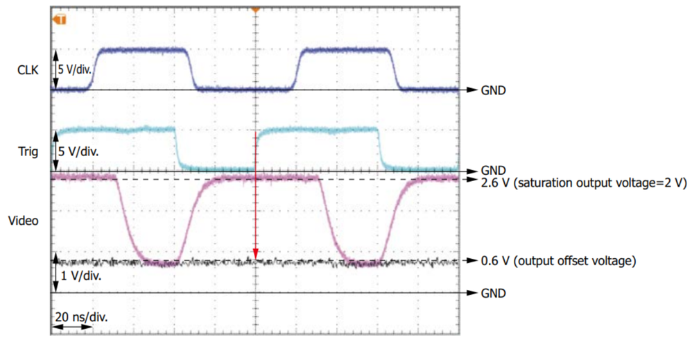
I am using a STM32H723ZG board for a project. In this project I must sample the signal coming from an image sensor that sends the pixel values as pulses with analog amplitudes. This sensor also provides a trigger signal so that the pixels data should be sampled at the rising edge of the trigger signal (an example is shown in the image below).

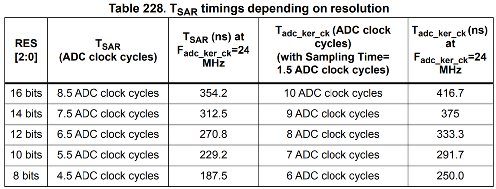
Based on the following table (available in the pg.1014 in the reference manual RM0468:(

The pixel pulses are sent with a frequency of 5 Mhz. For that reason I decided to use the two 16-bit ADCs with 12 bits resolution in alternate trigger mode. In this mode, both ADCs are triggered by an external signal alternately. So, in this way, I can read the signal at 5MHz.
The alternate trigger mode can only be implemented with injected channels (mentioned in the reference manual), which eliminates the possibility of using the DMA because DMA doesn't work with injected channels. So, I am using the ADCs with polling.
I am also calibrating the ADCs independently before starting them. However, there is a strange behaviour in the sampled signal after uploading the code. When I upload the code, I randomly get any of three possible outcomes:

My configurations for the ADCs are: For the ADC1:
  hadc1.Instance = ADC1;
  hadc1.Init.ClockPrescaler = ADC_CLOCK_ASYNC_DIV1;
  hadc1.Init.Resolution = ADC_RESOLUTION_12B;
  hadc1.Init.ScanConvMode = ADC_SCAN_DISABLE;
  hadc1.Init.EOCSelection = ADC_EOC_SINGLE_CONV;
  hadc1.Init.LowPowerAutoWait = DISABLE;
  hadc1.Init.ContinuousConvMode = DISABLE;
  hadc1.Init.NbrOfConversion = 1;
  hadc1.Init.DiscontinuousConvMode = DISABLE;
  hadc1.Init.ConversionDataManagement = ADC_CONVERSIONDATA_DR;
  hadc1.Init.Overrun = ADC_OVR_DATA_PRESERVED;
  hadc1.Init.LeftBitShift = ADC_LEFTBITSHIFT_NONE;
  hadc1.Init.OversamplingMode = DISABLE;
  if (HAL_ADC_Init(&hadc1) != HAL_OK)
  {
    Error_Handler();
  }

  /** Configure the ADC multi-mode
  */
  multimode.Mode = ADC_DUALMODE_ALTERTRIG;
  multimode.DualModeData = ADC_DUALMODEDATAFORMAT_DISABLED;
  multimode.TwoSamplingDelay = ADC_TWOSAMPLINGDELAY_1CYCLE;
  if (HAL_ADCEx_MultiModeConfigChannel(&hadc1, &multimode) != HAL_OK)
  {
    Error_Handler();
  }

  /** Disable Injected Queue
  */
  HAL_ADCEx_DisableInjectedQueue(&hadc1);

  /** Configure Injected Channel
  */
  sConfigInjected.InjectedChannel = ADC_CHANNEL_4;
  sConfigInjected.InjectedRank = ADC_INJECTED_RANK_1;
  sConfigInjected.InjectedSamplingTime = ADC_SAMPLETIME_8CYCLES_5;
  sConfigInjected.InjectedSingleDiff = ADC_SINGLE_ENDED;
  sConfigInjected.InjectedOffsetNumber = ADC_OFFSET_NONE;
  sConfigInjected.InjectedOffset = 0;
  sConfigInjected.InjectedNbrOfConversion = 1;
  sConfigInjected.InjectedDiscontinuousConvMode = DISABLE;
  sConfigInjected.AutoInjectedConv = DISABLE;
  sConfigInjected.QueueInjectedContext = DISABLE;
  sConfigInjected.ExternalTrigInjecConv = ADC_EXTERNALTRIGINJEC_EXT_IT15;
  sConfigInjected.ExternalTrigInjecConvEdge = ADC_EXTERNALTRIGINJECCONV_EDGE_RISING;
  sConfigInjected.InjecOversamplingMode = DISABLE;
For the ADC2:
  hadc2.Instance = ADC2;
  hadc2.Init.ClockPrescaler = ADC_CLOCK_ASYNC_DIV1;
  hadc2.Init.Resolution = ADC_RESOLUTION_12B;
  hadc2.Init.ScanConvMode = ADC_SCAN_DISABLE;
  hadc2.Init.EOCSelection = ADC_EOC_SINGLE_CONV;
  hadc2.Init.LowPowerAutoWait = DISABLE;
  hadc2.Init.ContinuousConvMode = DISABLE;
  hadc2.Init.NbrOfConversion = 1;
  hadc2.Init.DiscontinuousConvMode = DISABLE;
  hadc2.Init.ConversionDataManagement = ADC_CONVERSIONDATA_DR;
  hadc2.Init.Overrun = ADC_OVR_DATA_PRESERVED;
  hadc2.Init.LeftBitShift = ADC_LEFTBITSHIFT_NONE;
  hadc2.Init.OversamplingMode = DISABLE;
  if (HAL_ADC_Init(&hadc2) != HAL_OK)
  {
    Error_Handler();
  }

  /** Disable Injected Queue
  */
  HAL_ADCEx_DisableInjectedQueue(&hadc2);

  /** Configure Injected Channel
  */
  sConfigInjected.InjectedChannel = ADC_CHANNEL_4;
  sConfigInjected.InjectedRank = ADC_INJECTED_RANK_1;
  sConfigInjected.InjectedSamplingTime = ADC_SAMPLETIME_8CYCLES_5;
  sConfigInjected.InjectedSingleDiff = ADC_SINGLE_ENDED;
  sConfigInjected.InjectedOffsetNumber = ADC_OFFSET_NONE;
  sConfigInjected.InjectedOffset = 0;
  sConfigInjected.InjectedNbrOfConversion = 1;
  sConfigInjected.InjectedDiscontinuousConvMode = DISABLE;
  sConfigInjected.AutoInjectedConv = DISABLE;
  sConfigInjected.QueueInjectedContext = DISABLE;
  sConfigInjected.InjecOversamplingMode = DISABLE;
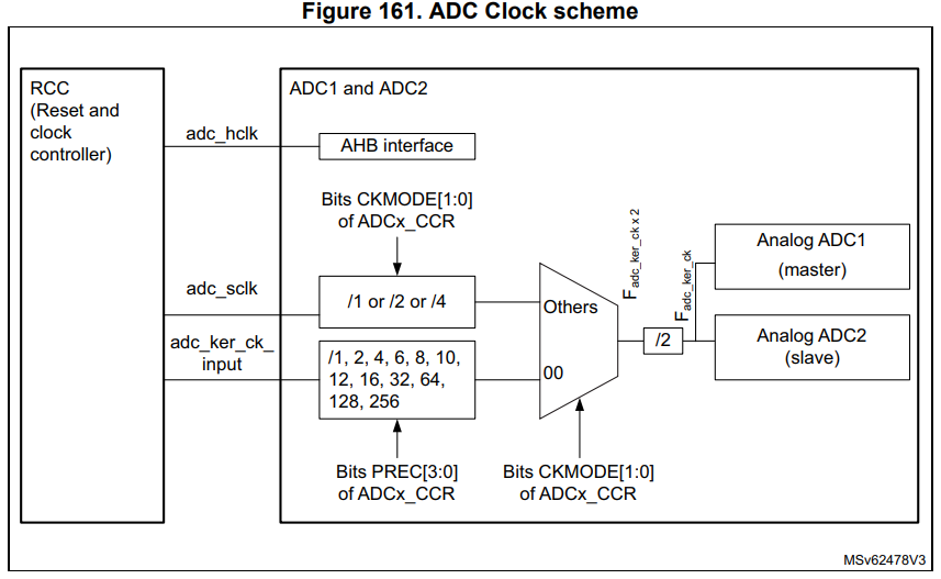
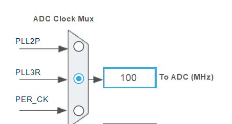
Finally, based on the datasheet, the maximum ADC frequency is 50 MHz. So to reach that value I checked the ADC clock scheme and there is a internal frequency divider that divides the frequency by 2 (see image below). Then, the divided frequency is used by the ADC (pg. 981, reference manual RM0468).


- Labels:
-
ADC
-
STM32CubeIDE
-
STM32CubeMX
-
STM32H7 Series
- Mark as New
- Bookmark
- Subscribe
- Mute
- Subscribe to RSS Feed
- Permalink
- Email to a Friend
- Report Inappropriate Content
2023-02-28 2:40 AM
The "result" waveforms, do they display a combined output from both ADCs? Can you display them independently?
JW
- Mark as New
- Bookmark
- Subscribe
- Mute
- Subscribe to RSS Feed
- Permalink
- Email to a Friend
- Report Inappropriate Content
2023-02-28 2:47 AM
Hi @Community member,
Yes, it looks like both ADCs follow the same pattern, but one has a different offset relative to the other and sometimes they have the same offset (as in the image of clause a)). Is it possible to always have the same offset for both?
CT
- Mark as New
- Bookmark
- Subscribe
- Mute
- Subscribe to RSS Feed
- Permalink
- Email to a Friend
- Report Inappropriate Content
2023-02-28 4:22 AM
Offset may be result of different calibration. You can observe the calibration results in the CALFACT registers. You can even change them, although wouldn't recommend that, and I'd personally strive to find the primary source of the differences, if there are any.
Note, that the primary requirement for any serious ADC work, including calibration, is rock stable VREF+ against VREF-/VSSA (which includes VREF+ source, VREF+ and VREF-/VSSA routing including its "quietness" and decoupling from digital VSS, recommended or more decoupling capacitors' combo between VREF+ and VREF-/VSSA at the absolute minimal distance, etc. We are talking millivolts or better here. VREF+ is subject to similar pulsed current consumption from the switched capacitors as ADC inputs are, and its impact on ADC measurement results is huge.
JW
- Readout external ADC by SPI doesn't work correctly in STM32CubeIDE (MCUs)
- STM32F103x strange behavior using HAL_RTC_GetTime() together with RTC interrupts (ALR and SEC flags) in STM32CubeIDE (MCUs)
- Issue with SPI2/DMA in Receives only for STM32L476RG (Nucleo) via LL Template. in STM32CubeMX (MCUs)
- I2C conflict with timer output in STM32CubeMX (MCUs)