- STMicroelectronics Community
- STM32 MCUs
- STM32 MCUs Products
- Re: Work with FSMC and two devices, problems with ...
- Subscribe to RSS Feed
- Mark Topic as New
- Mark Topic as Read
- Float this Topic for Current User
- Bookmark
- Subscribe
- Mute
- Printer Friendly Page
Work with FSMC and two devices, problems with choosing one device
- Mark as New
- Bookmark
- Subscribe
- Mute
- Subscribe to RSS Feed
- Permalink
- Email to a Friend
- Report Inappropriate Content
2020-01-27 08:44 PM
Hello,
My program uses two FSMC_Bank1 for the tft screen and memory (62WV51216ALL), NORSRAM3 is used for memory and NORSRAM4 for the screen, a problem has been identified that when accessing NORSRAM3 (memory), the CS signal (FSMC_NE3) goes low and remains so permanently. The same thing happens with the signal for the CS screen (FSMC_NE4) and when garbage from points are written to the memory on the screen. How can I return the CS signals to their normal position after accessing the right data source?
Solved! Go to Solution.
- Labels:
-
FMC-FSMC
-
STM32F4 Series
Accepted Solutions
- Mark as New
- Bookmark
- Subscribe
- Mute
- Subscribe to RSS Feed
- Permalink
- Email to a Friend
- Report Inappropriate Content
2020-01-29 04:15 AM
At this point I'm out of ideas.
You may want to try to ask for help ST directly through the web support form.
JW
- Mark as New
- Bookmark
- Subscribe
- Mute
- Subscribe to RSS Feed
- Permalink
- Email to a Friend
- Report Inappropriate Content
2020-01-27 10:45 PM
STM32F407ZET
init SRAM
  readWriteTiming.FSMC_AddressSetupTime = 0x0F;
  readWriteTiming.FSMC_AddressHoldTime = 0x02;
  readWriteTiming.FSMC_DataSetupTime = 0x0F;
  readWriteTiming.FSMC_BusTurnAroundDuration = 0x00;
  readWriteTiming.FSMC_CLKDivision = 0x00;
  readWriteTiming.FSMC_DataLatency = 0x00;
  readWriteTiming.FSMC_AccessMode = FSMC_AccessMode_B;


  FSMC_NORSRAMInitStructure.FSMC_Bank = FSMC_Bank1_NORSRAM3;
  FSMC_NORSRAMInitStructure.FSMC_DataAddressMux = FSMC_DataAddressMux_Disable;
  FSMC_NORSRAMInitStructure.FSMC_MemoryType =FSMC_MemoryType_SRAM;// FSMC_MemoryType_SRAM;  //SRAM
  FSMC_NORSRAMInitStructure.FSMC_MemoryDataWidth = FSMC_MemoryDataWidth_16b;
  FSMC_NORSRAMInitStructure.FSMC_BurstAccessMode =FSMC_BurstAccessMode_Disable;// FSMC_BurstAccessMode_Disable;
  FSMC_NORSRAMInitStructure.FSMC_WaitSignalPolarity = FSMC_WaitSignalPolarity_Low;
  FSMC_NORSRAMInitStructure.FSMC_AsynchronousWait=FSMC_AsynchronousWait_Disable;
  FSMC_NORSRAMInitStructure.FSMC_WrapMode = FSMC_WrapMode_Disable;
  FSMC_NORSRAMInitStructure.FSMC_WaitSignalActive = FSMC_WaitSignalActive_BeforeWaitState;
  FSMC_NORSRAMInitStructure.FSMC_WriteOperation = FSMC_WriteOperation_Enable;
  FSMC_NORSRAMInitStructure.FSMC_WaitSignal = FSMC_WaitSignal_Disable;
  FSMC_NORSRAMInitStructure.FSMC_ExtendedMode = FSMC_ExtendedMode_Enable;
  FSMC_NORSRAMInitStructure.FSMC_WriteBurst = FSMC_WriteBurst_Disable;
  FSMC_NORSRAMInitStructure.FSMC_ReadWriteTimingStruct = &readWriteTiming;
  FSMC_NORSRAMInitStructure.FSMC_WriteTimingStruct = &readWriteTiming;
  FSMC_NORSRAMInit(&FSMC_NORSRAMInitStructure);

 	FSMC_NORSRAMCmd(FSMC_Bank1_NORSRAM3, ENABLE);  // BANK3
init TFT
readWriteTiming.FSMC_AddressSetupTime = 0XF;	 // 1/168M=6ns*16=96ns
  readWriteTiming.FSMC_AddressHoldTime = 0x00;
  readWriteTiming.FSMC_DataSetupTime = 24;			//6*25=150ns
  readWriteTiming.FSMC_BusTurnAroundDuration = 0x00;
  readWriteTiming.FSMC_CLKDivision = 0x00;
  readWriteTiming.FSMC_DataLatency = 0x00;
  readWriteTiming.FSMC_AccessMode = FSMC_AccessMode_A;


	writeTiming.FSMC_AddressSetupTime =8;	      //ַ֘HCLK =48ns
  writeTiming.FSMC_AddressHoldTime = 0x00;
  writeTiming.FSMC_DataSetupTime = 8;		 //HCLK=54ns
  writeTiming.FSMC_BusTurnAroundDuration = 0x00;
  writeTiming.FSMC_CLKDivision = 0x00;
  writeTiming.FSMC_DataLatency = 0x00;
  writeTiming.FSMC_AccessMode = FSMC_AccessMode_A;


  FSMC_NORSRAMInitStructure.FSMC_Bank = FSMC_Bank1_NORSRAM4;
  FSMC_NORSRAMInitStructure.FSMC_DataAddressMux = FSMC_DataAddressMux_Disable;
  FSMC_NORSRAMInitStructure.FSMC_MemoryType =FSMC_MemoryType_SRAM;// FSMC_MemoryType_SRAM;  //SRAM
  FSMC_NORSRAMInitStructure.FSMC_MemoryDataWidth = FSMC_MemoryDataWidth_16b;
  FSMC_NORSRAMInitStructure.FSMC_BurstAccessMode =FSMC_BurstAccessMode_Disable;// FSMC_BurstAccessMode_Disable;
  FSMC_NORSRAMInitStructure.FSMC_WaitSignalPolarity = FSMC_WaitSignalPolarity_Low;
	FSMC_NORSRAMInitStructure.FSMC_AsynchronousWait=FSMC_AsynchronousWait_Disable;
  FSMC_NORSRAMInitStructure.FSMC_WrapMode = FSMC_WrapMode_Disable;
  FSMC_NORSRAMInitStructure.FSMC_WaitSignalActive = FSMC_WaitSignalActive_BeforeWaitState;
  FSMC_NORSRAMInitStructure.FSMC_WriteOperation = FSMC_WriteOperation_Enable;
  FSMC_NORSRAMInitStructure.FSMC_WaitSignal = FSMC_WaitSignal_Disable;
  FSMC_NORSRAMInitStructure.FSMC_ExtendedMode = FSMC_ExtendedMode_Enable;
  FSMC_NORSRAMInitStructure.FSMC_WriteBurst = FSMC_WriteBurst_Disable;
  FSMC_NORSRAMInitStructure.FSMC_ReadWriteTimingStruct = &readWriteTiming;
  FSMC_NORSRAMInitStructure.FSMC_WriteTimingStruct = &writeTiming;

  FSMC_NORSRAMInit(&FSMC_NORSRAMInitStructure);

FSMC_NORSRAMCmd(FSMC_Bank1_NORSRAM4, ENABLE); // BANK1 - Mark as New
- Bookmark
- Subscribe
- Mute
- Subscribe to RSS Feed
- Permalink
- Email to a Friend
- Report Inappropriate Content
2020-01-28 12:16 AM
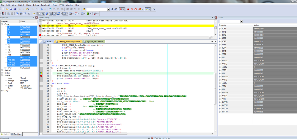
Read out and check/post content of FSMC registers.
JW
- Mark as New
- Bookmark
- Subscribe
- Mute
- Subscribe to RSS Feed
- Permalink
- Email to a Friend
- Report Inappropriate Content
2020-01-28 04:36 AM
По�?ле запи�?и в пам�?ть
- Mark as New
- Bookmark
- Subscribe
- Mute
- Subscribe to RSS Feed
- Permalink
- Email to a Friend
- Report Inappropriate Content
2020-01-28 06:38 AM
This looks to be OK, I don't see anything obviously wrong here.
If you use the two peripherals separately (i.e. initialize only one of them in FSMC) they work OK?
Try to disable Bank1.
JW
- Mark as New
- Bookmark
- Subscribe
- Mute
- Subscribe to RSS Feed
- Permalink
- Email to a Friend
- Report Inappropriate Content
2020-01-28 08:08 PM
Hello,
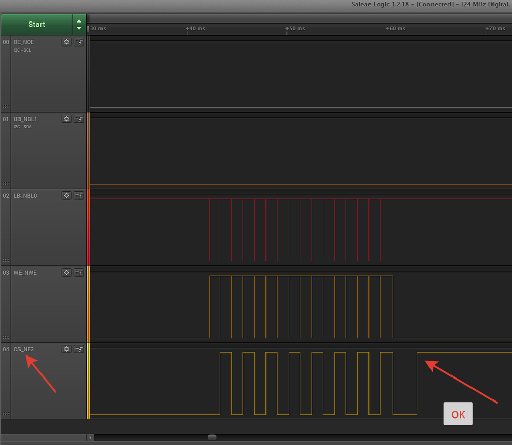
when one of the devices is turned off, the behavior of the CS (NE3 or NE4) signals becomes normal. disconnected separately the memory on the NE 4 logical analyzer; SWITCHED NORMALLY; turned off the screen (by setting comments on the screen); NE 3 switching is normal (attachment). The combined operation of the screen and memory causes a single change in the signal from 1 -> 0 at the outputs of NE 3 and NE 4
- Mark as New
- Bookmark
- Subscribe
- Mute
- Subscribe to RSS Feed
- Permalink
- Email to a Friend
- Report Inappropriate Content
2020-01-28 08:47 PM
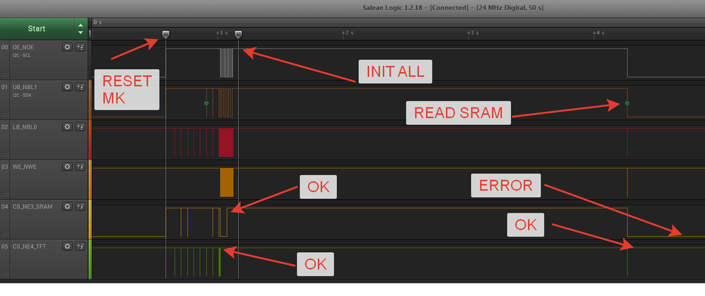
Changed the initialization order, at the beginning of the screen then the memory. The screen selection signal NE 4 now works fine. BUT the memory selection signal does not work. In the attachment, the screen from the moment the microcontroller resets.
Maybe something is wrong with the memory access? I give all the pieces of the appeal code:
void fsmc_sram_test_1(void)
{   u16 temp=0;
    fsmc_sram_test_write(0x0000,0xBBAA);
    temp=fsmc_sram_test_read(0X0000);
    LCD_ShowxNum(60,190,temp,6,16,0);
    printf("Data SINGL:%x\r\n",temp);
}
/*****************************************************/
void FSMC_SRAM_WriteBuffer(u16* pBuffer,u32 WriteAddr,u32 n)
{
	for(;n!=0;n--)
	{
		*(vu16*)(Bank1_SRAM3_ADDR+WriteAddr)=*pBuffer;
		WriteAddr++;
		pBuffer++;
	}
}
/*****************************************************/
void FSMC_SRAM_ReadBuffer(u16* pBuffer,u32 ReadAddr,u32 n)
{
	for(;n!=0;n--)
	{
		*pBuffer++=*(vu16*)(Bank1_SRAM3_ADDR+ReadAddr);
		ReadAddr++;
	}
}
/*****************************************************/
void fsmc_sram_test_write(u32 addr,u16 data)
{
	FSMC_SRAM_WriteBuffer(&data,addr,1);
}
/*****************************************************/
u16 fsmc_sram_test_read(u32 addr)
{
	u16 data;
	FSMC_SRAM_ReadBuffer(&data,addr,1);
	return data;
}- Mark as New
- Bookmark
- Subscribe
- Mute
- Subscribe to RSS Feed
- Permalink
- Email to a Friend
- Report Inappropriate Content
2020-01-28 09:37 PM
Compulsory measures to return the signal have no effect :(
    *(vu16*)(Bank1_SRAM3_ADDR+0x0000)=0xBBAA;
 GPIO_PinAFConfig(GPIOG,GPIO_PinSource10,GPIO_AF_RTC_50Hz);
 GPIO_SetBits(GPIOG, GPIO_Pin_10);
 GPIO_PinAFConfig(GPIOG,GPIO_PinSource10,GPIO_AF_FSMC);
In the simulator, everything is fine and in the iron there is no reaction to these actions.
- Mark as New
- Bookmark
- Subscribe
- Mute
- Subscribe to RSS Feed
- Permalink
- Email to a Friend
- Report Inappropriate Content
2020-01-29 12:10 AM
Did you try to disable FSMC Bank1?
JW
- Mark as New
- Bookmark
- Subscribe
- Mute
- Subscribe to RSS Feed
- Permalink
- Email to a Friend
- Report Inappropriate Content
2020-01-29 12:23 AM
I do not understand why disable FSMC Bank1?
I turned off the devices one at a time and the selection line began to work in both cases. The collaboration of the devices is incorrect, but turning off FSMC Bank1 how will I work with a memory chip and a screen? Separately, port Port G -> pin 10 switches normally without problems.
- USB endpoint limitations? in STM32 MCUs Products
- No device found on target (SWD connection) in STM32 MCUs Products
- USB Device Not Recognized Using USB3300 PHY on STM32 Nucleo-F446ZE in STM32 MCUs Products
- Dependencies issue when installing STM32CubeCLT v16.0.0 in STM32CubeIDE (MCUs)
- Problems with SPI3 on STM32H725ZGT6 device in STM32 MCUs Products


