- STMicroelectronics Community
- STM32 MCUs
- STM32 MCUs Products
- Re: [SILICON BUG?] STM32F3 DAC has 4LSB sawtooth w...
- Subscribe to RSS Feed
- Mark Topic as New
- Mark Topic as Read
- Float this Topic for Current User
- Bookmark
- Subscribe
- Mute
- Printer Friendly Page
[SILICON BUG?] STM32F3 DAC has 4LSB sawtooth with 1 minute period
- Mark as New
- Bookmark
- Subscribe
- Mute
- Subscribe to RSS Feed
- Permalink
- Email to a Friend
- Report Inappropriate Content
2019-10-30 9:11 AM
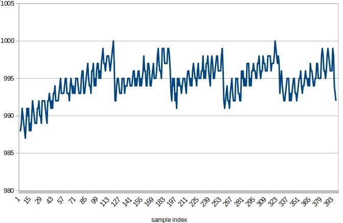
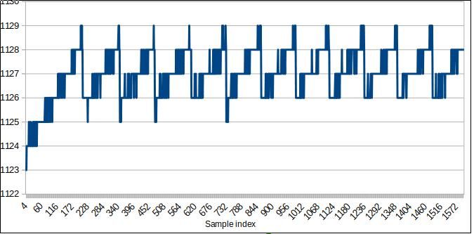
Over the past month, I've been trying to figure out if the DAC in the STM32F3 actually has a silicon bug. I observe a sawtooth with an approx 1 minute period in the DAC output (as measured by the ADC on the same chip). The first large "tooth" is always ~2mins long, then the period is roughly 1minute after that. Here's an example of what I mean:
Here are a few lines of inquiry I have eliminated so far:
Is it [your choise of something that causes noise]? No, it's regular and predictable. Noise by definition is random. The little jitters are noise; the 4 LSB sawteeth are not noise.
Is it the board? No, I observe this in boards of my own design and my F334R8 nucleo board.
Is it the specific chip or family? No, I observe this in several F334K6, F334K8 and F334R8 chips so far.
Is it the specific power supply? No, I observe it when the MCU is fed by LP5951 LDO on my board, and also whatever LDO the nucleo board uses. My board supply is correctly decoupled with 4.4uF at supply + 100nF adjacent to all VDD and VDDA pins.
Is it due to DMA driver? No, you can also see this using HAL_DAC_SetValue().
Is it due to EM interference in your lab? No, I still see the sawtooth when I change to laptop and run everything in my basement.
How do you know it's the DAC outputting a sawtooth ripple values and not the ADC adding a sawtooth ripple to its readings? Because I tested the ADC with a 1.5V battery several times (even with the DAC running but the DAC pin disconnected) and it measures very stable values with only 1LSB of noise; no sawtooth.
Is it due to the DAC channel? No, I tried DAC1 ch1 and ch2. They both have sawtooth.
So now I'm stuck. As far as I can tell, there is no reason for the DAC to be emitting a sawtooth except due to some internal Vref problem inside the chip. Can you please confirm?
I've posted a main.c here which can be used as template code for confirming. Connect PA0 (ADC1 ch1) and PA4 (ADC2 ch1) to PA5 (DAC1 ch2). Configure using the prior release STM32F3 HAL (your latest release for STMCubeIDE 1.1.0 has an ADC software bug too, see my other recent post). ADC1 & ADC2 in dual simultaneous mode, DAC using DMA and TIM6 as trigger (or without DMA also snows sawtooth, at your option). SWV trace enabled. 64MHz HSI PLL clock.
Obviously the DAC op amp doesn't have the GBW to overcome the ADC kickback voltage drop so the values will be lower than outputted by the DAC, but you'll see the sawtooth effect printed in the ITM console.
- Labels:
-
ADC
-
Bug-report
-
DAC
-
STM32F3 Series
- Mark as New
- Bookmark
- Subscribe
- Mute
- Subscribe to RSS Feed
- Permalink
- Email to a Friend
- Report Inappropriate Content
2019-10-30 12:17 PM
10 Digits at 12 bit at 3 Volt range is several Millivolt. Did you cross check with a good voltmeter?
- Mark as New
- Bookmark
- Subscribe
- Mute
- Subscribe to RSS Feed
- Permalink
- Email to a Friend
- Report Inappropriate Content
2019-10-30 3:10 PM
Yes, the sawtooth was visible with a voltmeter under certain circumstances. That caused me to test a range of impedances (because I noticed that I could make the period vary while I was measuring with the voltmeter for some impedances), which makes me think it was an issue of the buffer op amp stability. I disabled the buffer and ran it with a really low resistive load and that was pretty stable, and then renabled and the output became stable under a variety of loads. Then I disabled it again and it connected the DAC directly to the ADC and it was still stable. So it can't be a silicon bug if I can stabilize it like that, and I now think I must have somehow screwed up an internal capacitor that caused an integration effect ... I'm at a bit of a loss to explain this one.
- Mark as New
- Bookmark
- Subscribe
- Mute
- Subscribe to RSS Feed
- Permalink
- Email to a Friend
- Report Inappropriate Content
2019-10-31 12:09 AM
If the reference voltage moves, the output would move, too.
And, you don't have a periodic once-per-minute task by chance, that could impact power consumption ?
- Mark as New
- Bookmark
- Subscribe
- Mute
- Subscribe to RSS Feed
- Permalink
- Email to a Friend
- Report Inappropriate Content
2019-10-31 2:07 AM
Change in reference voltage would be compensated in the ADC readings too though. No periodic tasks, just a basic program that sets the DAC output and then gets ADC readings every second or so.
The thing is that with the buffer dissabled the DAC is not behaving like an R2R ladder at all. I've read the application note, but it doesn't detail what's going on with the DAC internals enough for me to understand why the integrator effect occurs.
- Mark as New
- Bookmark
- Subscribe
- Mute
- Subscribe to RSS Feed
- Permalink
- Email to a Friend
- Report Inappropriate Content
2019-11-02 5:10 AM
> Change in reference voltage would be compensated in the ADC readings too though.
In the ideal world, yes. In reality, on ADC, you have some sampling process resulting in a current spike (which of course have also its consequences at least through the common ground) and then some switched-capacitors data conversion; and an unknown mechanism on the DAC side, which perhaps may be of switched-capacitors nature, too, e.g. running from an independent internal RC oscillator (I am speculating wildly here). That might result in all sorts of patterns, depending on mutual "synchronicity".
I don't say this is directly related to what you've observed, but see e.g. the Possible voltage drop caused by a transitory phase when the ADC is switching from a regular channel to an injected channel Rank 1 erratum in the 'F303x6/x8 errata.
JW
- Mark as New
- Bookmark
- Subscribe
- Mute
- Subscribe to RSS Feed
- Permalink
- Email to a Friend
- Report Inappropriate Content
2019-11-02 12:55 PM
ADC is fast and unfiltered DAC output probably isn't ideal DC line. Could it be aliasing because of some similar but not exact internal clocks?
You should look at this signal on oscilloscope and/or try some RC filter on DAC output.
- Mark as New
- Bookmark
- Subscribe
- Mute
- Subscribe to RSS Feed
- Permalink
- Email to a Friend
- Report Inappropriate Content
2019-11-03 11:42 AM
OK, I did more testing over the weekend with the Nucleo board and a wide range of impedances and filters connected to DAC1OUT (unbuffered). I've basically come to the conclusion that the DAC won't be stable unless there's a very good approximation of infinite impedance across all relevant frequencies at the terminal when the internal voltage follower op amp is not enabled (or more realistically, not available if you're not using DAC1Ch1). This includes my usage case: not working when connected directly to a 2nd-order active filter:
That degree of extraneous inaccuracy is OK for toys & music, but not for precision measurement work.
Both the inverting and voltage follower configs in AN4566 work, but I haven't found another useful config that's reliably stable. Unfortunately modelling the DAC as an R2R ladder is therefore not accurate, and I really wish ST had included such details about stability in their application note documentation because it would have saved me a lot of wasted time debugging my own DSP algorithms and my board designs.
- Mark as New
- Bookmark
- Subscribe
- Mute
- Subscribe to RSS Feed
- Permalink
- Email to a Friend
- Report Inappropriate Content
2019-11-03 12:21 PM
Do you observe the "sawtooth" (using an external measurement method) also if you switch the ADC completely off?
JW
- Mark as New
- Bookmark
- Subscribe
- Mute
- Subscribe to RSS Feed
- Permalink
- Email to a Friend
- Report Inappropriate Content
2019-11-11 2:44 AM
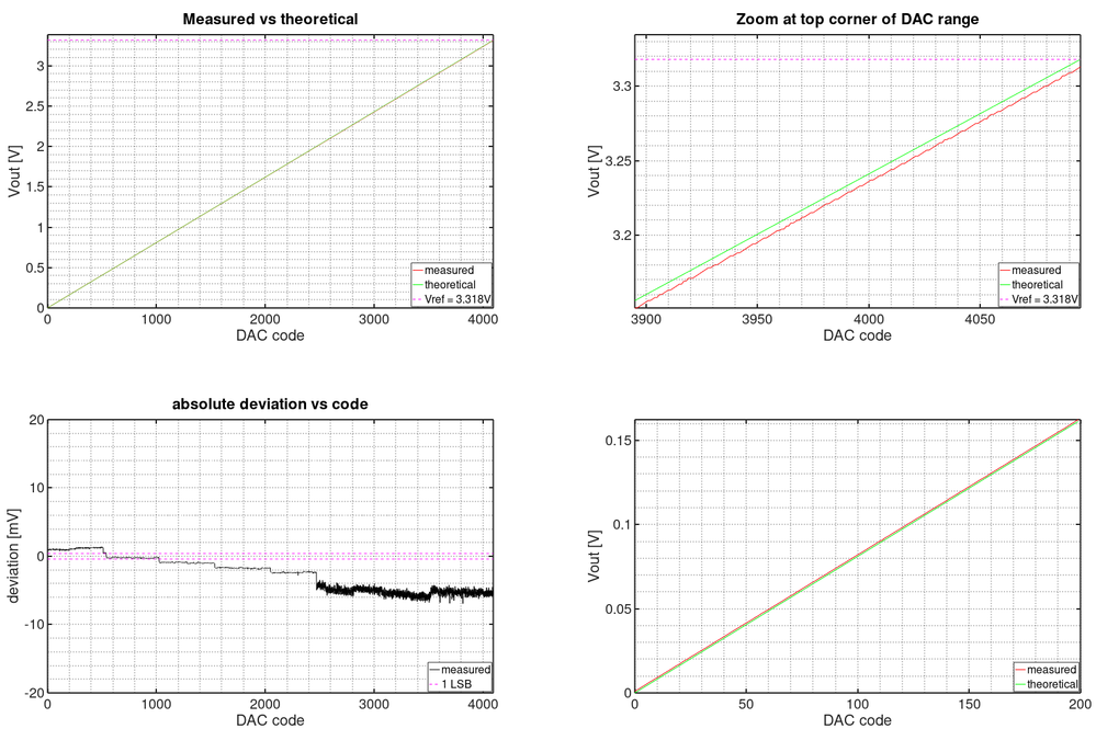
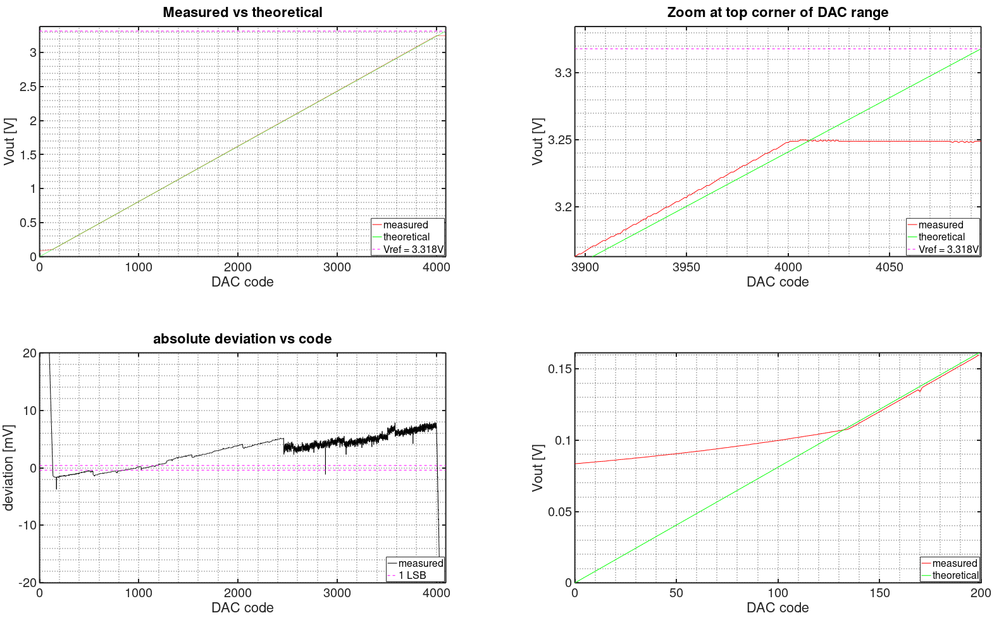
May be it can help you. About a year ago i've tested DAC at STM32F303K8 (Nuclo 32 board) with UT71A multimeter (~0.1%) with these results:
Without output buffer to High impedance (multimeter)
and with (internal) output buffer to 27k/27k divider (VDD/GND)
Measurment takes about 25 minutes (MCU reads data from multimeter by its optocoupled output). In left bottom graph is deviation from ideal state. AVDD was 3.3V (from voltage regulator on Nucleo board). Noise in range over 2V is due multimeter range (switch from 2V to 20V range). Of course i've measured "ramp" signal, but your "tooths" should be visible with amplitude about ~2.4mV. That problem with high probability didnt show up at F303K8. I recommended do measurment against voltmetr.
Good luck.


