- STMicroelectronics Community
- STM32 MCUs
- STM32 MCUs Products
- Re: STM32H74x Errata 2.5.3 QuadSPI - is the provid...
- Subscribe to RSS Feed
- Mark Topic as New
- Mark Topic as Read
- Float this Topic for Current User
- Bookmark
- Subscribe
- Mute
- Printer Friendly Page
STM32H74x Errata 2.5.3 QuadSPI - is the provided workaround feasible for read operation ?
- Mark as New
- Bookmark
- Subscribe
- Mute
- Subscribe to RSS Feed
- Permalink
- Email to a Friend
- Report Inappropriate Content
2020-05-30 03:23 AM
The errata suggest to "insert a dummy phase with at least two dummy cycles" when using indirect data read mode.
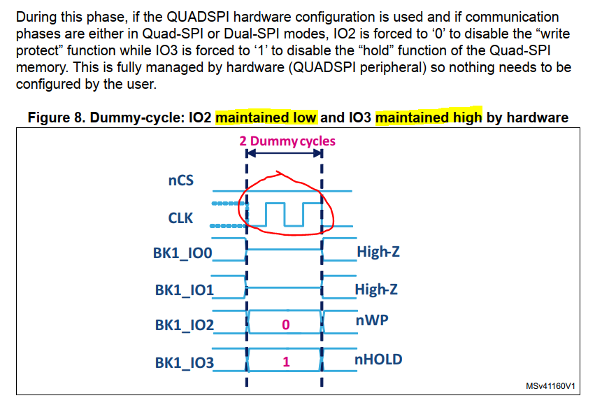
However, according to the documentation of the dummy cycle phase (AN4760 rev 3, section 3.1.4 and figure 8 ) states that in the dummy phase the clock continues to oscillate. So if used during read transaction, the data would be clocked in from the device and subsequently lost.
Moreover, the data lines 2 and 3 are driven during these cycles.
Am I reading this wrong, or is the workaround not suitable for the intended purpose of read operation ?
- Labels:
-
Documentation
-
QSPI
-
STM32H7 Series
- Mark as New
- Bookmark
- Subscribe
- Mute
- Subscribe to RSS Feed
- Permalink
- Email to a Friend
- Report Inappropriate Content
2020-05-30 04:11 AM
From the RM: "The QUADSPI is a specialized communication interface targeting single, dual or quad SPI Flash memories."
For a flash memory, indirect read with data phase only makes little sense, even in so-called XIP-mode at least address phase is required additionally.
So the problem does appear only if the QSPI is used in a way it was not designed for ...
- Mark as New
- Bookmark
- Subscribe
- Mute
- Subscribe to RSS Feed
- Permalink
- Email to a Friend
- Report Inappropriate Content
2020-05-31 11:46 AM
Well, if implemented as designed (without the errata bugs), it would have been extremely useful in interfacing to modern multi-lane ADC and DAC ICs.
probably the only option as is would be to switch to different CPU or insert FPGA in the middle :unamused_face:
- Mark as New
- Bookmark
- Subscribe
- Mute
- Subscribe to RSS Feed
- Permalink
- Email to a Friend
- Report Inappropriate Content
2020-06-01 12:30 AM
There are 10 SPI interfaces (counting USARTs too) on the STM32H743, how many channels do you need?
Reading GPIO->IDR with DMA triggered by a timer which also provides the clock on a PWM output, or receives the external clock signal on a capture input would work too.
I think FMC too could be abused to provide a multi-channel spi like interface, but the "clock" phase might be wrong. An external inverter could cure that though.
- Accessing calibration values with ICACHE enabled causes hard fault in STM32 MCUs Products
- STM32F415 DMA SPI transfer after stop mode in STM32 MCUs Products
- [bugs/caveats/misc fixes] STM32H7S Cube in STM32CubeMX (MCUs)
- ethernet stopping.... after running 30 to 48 hours continuously. in STM32CubeMX (MCUs)
- ST-Link-V3 on MacBook Pro M2 running Sonoma 14.4 only works through hub in STM32 MCUs Boards and hardware tools

