- STMicroelectronics Community
- STM32 MCUs
- STM32 MCUs Products
- Re: Questions regarding ADC ON STM32
- Subscribe to RSS Feed
- Mark Topic as New
- Mark Topic as Read
- Float this Topic for Current User
- Bookmark
- Subscribe
- Mute
- Printer Friendly Page
Questions regarding ADC ON STM32
- Mark as New
- Bookmark
- Subscribe
- Mute
- Subscribe to RSS Feed
- Permalink
- Email to a Friend
- Report Inappropriate Content
2022-04-25 04:51 AM
Hi All,
I'm starting to get familiar with the STM32 Series of Microprocessors and I'm completing some exercises using a mixture of direct writting to peripherals and low level ST libraries using the CUBEMX to get familiar with the chips. I'm using the Nucleo -F072RB
At this point I stumbled across a challenge, regarding the ADC module. I don't seem to be able to read the values on chanel 2 and 3 (PA2 and PA3).
Using the code below I can read PB0 (Channel 8) just fine. I ave also tried to read te internal temperatre sensor and reference and they seem to work fine. Any ideas why the inputs at PORTA don't work?
My code to read the ADC is as follows:
...
  ADC1->CHSELR = (ADC_CHSELR_CHSEL3);
  while (1)
  {
  		ADC1->SMPR = 7;                                                                 // Sample Time
  		ADC1->CFGR1 &= ~ ADC_CFGR1_CONT;				// Discontinuous mode
  		ADC1->CR |= ADC_CR_ADEN | ADC_CR_ADSTART;

while ((ADC1->ISR & ADC_ISR_EOC) == 0) /* Wait end of conversion */
        {
        ADC_Result[1] = ADC1->DR; /* Store the ADC conversion result */
        }
  }
This is my ADC init code:
/* USER CODE BEGIN Header */
/**
  ******************************************************************************
  * @file    adc.c
  * @brief   This file provides code for the configuration
  *          of the ADC instances.
  ******************************************************************************
  * @attention
  *
  * Copyright (c) 2022 STMicroelectronics.
  * All rights reserved.
  *
  * This software is licensed under terms that can be found in the LICENSE file
  * in the root directory of this software component.
  * If no LICENSE file comes with this software, it is provided AS-IS.
  *
  ******************************************************************************
  */
/* USER CODE END Header */
/* Includes ------------------------------------------------------------------*/
#include "adc.h"

/* USER CODE BEGIN 0 */

/* USER CODE END 0 */

/* ADC init function */
void MX_ADC_Init(void)
{

  /* USER CODE BEGIN ADC_Init 0 */

  /* USER CODE END ADC_Init 0 */

  LL_ADC_InitTypeDef ADC_InitStruct = {0};
  LL_ADC_REG_InitTypeDef ADC_REG_InitStruct = {0};

  LL_GPIO_InitTypeDef GPIO_InitStruct = {0};

  /* Peripheral clock enable */
  LL_APB1_GRP2_EnableClock(LL_APB1_GRP2_PERIPH_ADC1);

  LL_AHB1_GRP1_EnableClock(LL_AHB1_GRP1_PERIPH_GPIOA);
  LL_AHB1_GRP1_EnableClock(LL_AHB1_GRP1_PERIPH_GPIOB);
  /**ADC GPIO Configuration
  PA2   ------> ADC_IN2
  PA3   ------> ADC_IN3
  */
  GPIO_InitStruct.Pin = LL_GPIO_PIN_2;
  GPIO_InitStruct.Mode = LL_GPIO_MODE_ANALOG;
  GPIO_InitStruct.Pull = LL_GPIO_PULL_NO;
  LL_GPIO_Init(GPIOA, &GPIO_InitStruct);

  GPIO_InitStruct.Pin = LL_GPIO_PIN_3;
  GPIO_InitStruct.Mode = LL_GPIO_MODE_ANALOG;
  GPIO_InitStruct.Pull = LL_GPIO_PULL_NO;
  LL_GPIO_Init(GPIOA, &GPIO_InitStruct);

  GPIO_InitStruct.Pin = LL_GPIO_PIN_0;
  GPIO_InitStruct.Mode = LL_GPIO_MODE_ANALOG;
  GPIO_InitStruct.Pull = LL_GPIO_PULL_NO;
  LL_GPIO_Init(GPIOB, &GPIO_InitStruct);

  /* USER CODE BEGIN ADC_Init 1 */

  /* USER CODE END ADC_Init 1 */

  LL_ADC_REG_SetSequencerChAdd(ADC1, LL_ADC_CHANNEL_8);
  /** Configure Regular Channel
  */
  LL_ADC_REG_SetSequencerChAdd(ADC1, LL_ADC_CHANNEL_2);

  /** Configure Regular Channel
  */
  LL_ADC_REG_SetSequencerChAdd(ADC1, LL_ADC_CHANNEL_3);

  /** Configure the global features of the ADC (Clock, Resolution, Data Alignment and number of conversion)
  */
  ADC_InitStruct.Clock = LL_ADC_CLOCK_ASYNC;
  ADC_InitStruct.Resolution = LL_ADC_RESOLUTION_12B;
  ADC_InitStruct.DataAlignment = LL_ADC_DATA_ALIGN_RIGHT;
  ADC_InitStruct.LowPowerMode = LL_ADC_LP_MODE_NONE;
  LL_ADC_Init(ADC1, &ADC_InitStruct);
  ADC_REG_InitStruct.TriggerSource = LL_ADC_REG_TRIG_SOFTWARE;
  ADC_REG_InitStruct.SequencerDiscont = LL_ADC_REG_SEQ_DISCONT_DISABLE;
  ADC_REG_InitStruct.ContinuousMode = LL_ADC_REG_CONV_SINGLE;
  ADC_REG_InitStruct.DMATransfer = LL_ADC_REG_DMA_TRANSFER_LIMITED;
  ADC_REG_InitStruct.Overrun = LL_ADC_REG_OVR_DATA_PRESERVED;
  LL_ADC_REG_Init(ADC1, &ADC_REG_InitStruct);
  LL_ADC_REG_SetSequencerScanDirection(ADC1, LL_ADC_REG_SEQ_SCAN_DIR_FORWARD);
  LL_ADC_SetSamplingTimeCommonChannels(ADC1, LL_ADC_SAMPLINGTIME_1CYCLE_5);
  /* USER CODE BEGIN ADC_Init 2 */

  /* USER CODE END ADC_Init 2 */

}

/* USER CODE BEGIN 1 */

/* USER CODE END 1 */
Solved! Go to Solution.
- Labels:
-
ADC
-
STM32F0 Series
Accepted Solutions
- Mark as New
- Bookmark
- Subscribe
- Mute
- Subscribe to RSS Feed
- Permalink
- Email to a Friend
- Report Inappropriate Content
2022-04-26 02:00 AM
Good news,
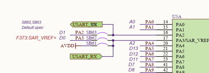
After sucess probing the the chip pins themselves, seems as the points on CN9/CN10 are left unconnected, on the nucleo board, by default (PA2/PA3 on CN9/CN10). A dig into the shematics shows a couple of test points, out of which SB62 and SB63 were left open.

Hope this can be helpfull for others.
- Mark as New
- Bookmark
- Subscribe
- Mute
- Subscribe to RSS Feed
- Permalink
- Email to a Friend
- Report Inappropriate Content
2022-04-26 02:00 AM
Good news,
After sucess probing the the chip pins themselves, seems as the points on CN9/CN10 are left unconnected, on the nucleo board, by default (PA2/PA3 on CN9/CN10). A dig into the shematics shows a couple of test points, out of which SB62 and SB63 were left open.

Hope this can be helpfull for others.
- Mark as New
- Bookmark
- Subscribe
- Mute
- Subscribe to RSS Feed
- Permalink
- Email to a Friend
- Report Inappropriate Content
2022-04-26 03:44 PM
while ((ADC1->ISR & ADC_ISR_EOC) == 0) /* Wait end of conversion */
{
    ADC_Result[1] = ADC1->DR; /* Store the ADC conversion result */
}
This does not do what you think it does and what comments say.
- Mark as New
- Bookmark
- Subscribe
- Mute
- Subscribe to RSS Feed
- Permalink
- Email to a Friend
- Report Inappropriate Content
2023-11-08 07:19 PM
SB62 is a memory adress or a physical connection, and how to access it
- CMake for TouchGFX via CubeMX? in STM32 VSCode extension (MCUs)
- LOAD ERROR: STM32 - read timeout 50062.0ms/50000ms in STM32CubeMX (MCUs)
- STM32CubeIDE Debug config in STM32CubeIDE (MCUs)
- SDCard with SDMMC on STM32H755ZI Nucleo in STM32 MCUs Embedded software
- NUCLEO-U5A5ZJ-Q with Riverdi RVA35HI in STM32 MCUs TouchGFX and GUI