- STMicroelectronics Community
- STM32 MCUs
- STM32 MCUs Products
- Re: M7 with 4xRAM ICs over FMC
- Subscribe to RSS Feed
- Mark Topic as New
- Mark Topic as Read
- Float this Topic for Current User
- Bookmark
- Subscribe
- Mute
- Printer Friendly Page
M7 with 4xRAM ICs over FMC
- Mark as New
- Bookmark
- Subscribe
- Mute
- Subscribe to RSS Feed
- Permalink
- Email to a Friend
- Report Inappropriate Content
2023-09-25 5:13 AM - edited 2023-09-26 11:18 PM
Hi,
We have a question about a system design we would like to implement for our product.
We are working with the STMF32F723 MCU and are developing our own HW. We need 216MByte of RAM for our application and would like to implement it with the functionality of DMA and FMC.
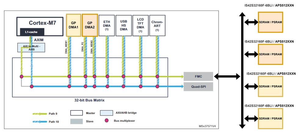
Here is a figure which shows the system architecture with the help of the graphic from application note AN4667.
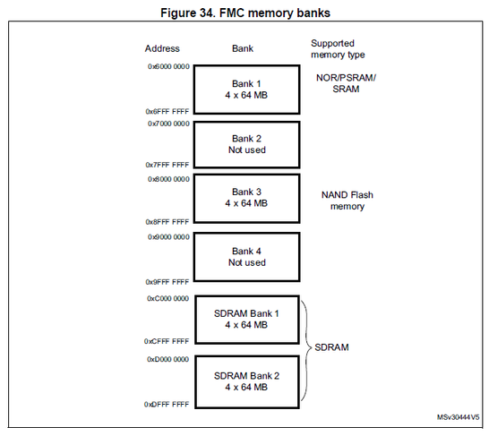
From the reference manual RM0431, we found following FMC memory bank map:
Now the question are:
- Is this system architecture possible at all?
- Could we use 4 blocks(64MByte) of PSRAM or also 4 Blocks(64MByte) of SDRAM?
- What are the benfits of SDRAM over PSRAM (which one is better for what?)
- Does it make sense, that two memory blocks are controlled over DM1 and the other two over DM2?
- So we can Read from one of the first two with DM1 and at the same time write to one of the oder two with DM2?
- What constraints do we need to consider when choosing the right RAM ic?
- Would the IS42S32160F-6BLI (SDRAM) or APS512XXN (PSRAM) both fit to the FMC of the M7 MCU?
Best regards,
Corsin
- Labels:
-
DMA
-
FMC-FSMC
-
RAM
-
STM32F7 Series
- Mark as New
- Bookmark
- Subscribe
- Mute
- Subscribe to RSS Feed
- Permalink
- Email to a Friend
- Report Inappropriate Content
2023-09-25 8:58 AM
Hello @CObri.1
Unfortunately, the architecture proposed is not possible. As referenced in RM0431, Bank 4 and 5 used to address SDRAM devices (1 device per bank).
To give better visibility on the answered topics, please click on Accept as Solution on the reply which solved your issue or answered your question.
- Mark as New
- Bookmark
- Subscribe
- Mute
- Subscribe to RSS Feed
- Permalink
- Email to a Friend
- Report Inappropriate Content
2023-09-26 11:07 PM - edited 2023-09-26 11:14 PM
Hello @FBL;,
Thanks for your answer, but it's still not clear for me. What I see is that only two SDRAM device are possible (Bank 4 one and Bank 5 one).
But with the PSRAM it should be not? In RM0431, on page 274 it is written following:
- From the FMC point of view, the external memory is divided into fixed-size banks of 256Mbytes each (see Figure34): • Bank 1 used to address up to 4 NOR Flash memory or PSRAM devices. This bank is split into 4 NOR/PSRAM subbanks with 4 dedicated chip selects, as follows:
Bank 1 - NOR/PSRAM 1
Bank 1 - NOR/PSRAM 2
Bank 1 - NOR/PSRAM 3
Bank 1 - NOR/PSRAM 4
I interpret this to imply that we can attach 4 external 64MByte PSRAM to the FMC bus.
What do I misunderstand?
Best Regards,
Corsin
- Mark as New
- Bookmark
- Subscribe
- Mute
- Subscribe to RSS Feed
- Permalink
- Email to a Friend
- Report Inappropriate Content
2023-09-26 11:28 PM
Hello @F.Belaid;,
Thanks for your answer, but it's still not clear for me. What I see is that only two SDRAM device are possible (Bank 4 one and Bank 5 one).
But with the PSRAM it should be not? In RM0431, on page 274 it is written following:
- From the FMC point of view, the external memory is divided into fixed-size banks of 256Mbytes each (see Figure34): • Bank 1 used to address up to 4 NOR Flash memory or PSRAM devices. This bank is split into 4 NOR/PSRAM subbanks with 4 dedicated chip selects, as follows:
Bank 1 - NOR/PSRAM 1
Bank 1 - NOR/PSRAM 2
Bank 1 - NOR/PSRAM 3
Bank 1 - NOR/PSRAM 4
I interpret this to imply that we can attach 4 external 64MByte PSRAM to the FMC bus.
What do I misunderstand?
Best Regards,
Corsin
- Mark as New
- Bookmark
- Subscribe
- Mute
- Subscribe to RSS Feed
- Permalink
- Email to a Friend
- Report Inappropriate Content
2023-09-28 2:37 AM
Hello again @CObri.1
- Each controller (SDRAM controller or PSRAM/NOR controller or NAND controller) has its signals and its configuration interface. Refer to figure 33 in the reference manual.
- It is possible to swap the mapping using SWP_FMC bit field in SYSCFG_MEMRMP register. However, you cannot use 4 SDRAM devices at the same time.
So, SDRAM bank1 and bank2 can be mapped at 0x6000 0000 and 0x7000 0000, but respectively NOR/PSRAM bank is mapped at 0xC000 0000 necessarily.
- Each SDRAM Bank can support memory devices with up to 4 internal Banks. But each bank has independent Chip Select and independent configuration.
I hope this helps!
To give better visibility on the answered topics, please click on Accept as Solution on the reply which solved your issue or answered your question.
- Mark as New
- Bookmark
- Subscribe
- Mute
- Subscribe to RSS Feed
- Permalink
- Email to a Friend
- Report Inappropriate Content
2023-10-09 1:24 AM
Hi,
Few comments about PSRAM
- APS512XXN is an Octal / Hexa RAM and is not supported on F7 / FMC memory controller, but would be most effective solution on SMT32H7,U5, H5, L5, L4+... for example. Key advantage of QSPI/OPI/HPI PSRAM versus legacy SDRAM are pin count, power, simplicity of design, space saving and especially for Hexa PSRAM versus SDRAMx32 competitiveness. Some illustrations at following links: https://www.st.com/en/partner-products-and-services/iot-ram-opi-psram.html and https://www.st.com/en/partner-products-and-services/iot-ram-hpi-opi-psram.html
- You can see some comparison of SDRAM/ADMUX PSRAM (FMC Memory controller) and OPI/QSPI PSRAM (Octal memory controller)
Alex
- Mark as New
- Bookmark
- Subscribe
- Mute
- Subscribe to RSS Feed
- Permalink
- Email to a Friend
- Report Inappropriate Content
2023-10-17 3:08 AM - edited 2023-10-17 7:47 AM
Dear @Alex - APMemory & @FBL
Thank you immensely for your assistance. Due to your help, we've been able to modify our requirements to a maximum RAM of 72 MBytes.
The revised architecture is as follows:
As a controller we still stick to the STMF32F723 controller
We plan to use the IS42/45S86400F, which has an internal design featuring 16M x 8 x 4 banks. Unfortunately, my search for SDRAM chips did not yield any options with 128MByte or 256MByte capacities. Are any of you aware of SDRAM chips that offer these higher memory sizes? Utilizing a single chip with a higher capacity would significantly simplify both hardware and firmware development.
Best regards, Corsin Obrist
- Mark as New
- Bookmark
- Subscribe
- Mute
- Subscribe to RSS Feed
- Permalink
- Email to a Friend
- Report Inappropriate Content
2023-10-17 4:17 AM
I can't see from your pic if you still stick to the F7. Be careful with that one concerning QSPI memory - it works, but not in memory mapped mode.
- Mark as New
- Bookmark
- Subscribe
- Mute
- Subscribe to RSS Feed
- Permalink
- Email to a Friend
- Report Inappropriate Content
2023-10-17 7:46 AM
Hi @LCE ,
Yes we still use the STMF32F723 controller.
So the two RAM Chips can be accessed (written/readout) over the FMC bus?
Best regards
Corsin
- Mark as New
- Bookmark
- Subscribe
- Mute
- Subscribe to RSS Feed
- Permalink
- Email to a Friend
- Report Inappropriate Content
2023-10-17 7:49 AM
Sorry, I have never used FMC.
I just had the (bad) experience that memory mapped read & write was not possible with a F767 and a QSPI RAM.


