- STMicroelectronics Community
- STM32 MCUs
- STM32 MCUs Products
- Re: Help to find a suitable configuration for PWM ...
- Subscribe to RSS Feed
- Mark Topic as New
- Mark Topic as Read
- Float this Topic for Current User
- Bookmark
- Subscribe
- Mute
- Printer Friendly Page
Help to find a suitable configuration for PWM + COMP + DAC
- Mark as New
- Bookmark
- Subscribe
- Mute
- Subscribe to RSS Feed
- Permalink
- Email to a Friend
- Report Inappropriate Content
2020-02-04 7:19 AM
Hi community,
I am struggling to find how (or if) is possible to use the TIM1 (advanced control timer) of the STM32FG071 to run a hysteretic current regulator completely in hardware (without relying on software)
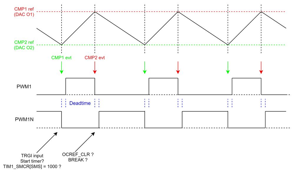
The idea is to use both comparators of the chip together with the 2 values of the DAC to set maximal e minimal current values, and then feed the current signal to the input of both comparators and let this information control the set /reset of the OC1 & OC1N outputs (to also take advantage of the deadtime), therefore controlling both frequency and duty cicle of the output stage.
As shown in this image:
The problem is that the due to the fairly complex control of this timer module and all its possible configurations I am not even able to conclude if it's feasible or not, I've already thought about using One Pulse Mode, OCREF_CLR, Gated mode and Break inputs, but the more I read the more complex it gets..
My question goes to the ones that are already experienced with the advanced parts of this timer, is this idea feasible? if yes, which features should I combine to put it to work?
OPM + OCREF_CLR ?
OPM + BRK ?
TRGI + OCREF_CLR ?
TRGI + BRK ?
what else could work ?
Thank you all in advance
Best Regards
Gustavo
- Labels:
-
COMP
-
DAC
-
STM32G0 Series
-
TIM
- Mark as New
- Bookmark
- Subscribe
- Mute
- Subscribe to RSS Feed
- Permalink
- Email to a Friend
- Report Inappropriate Content
2020-02-04 10:35 AM
I would try go for one COMP resetting the timer (and with appropriate PWM mode chosen setting OCx_REF) through either CH1 or CH2 or ETR, chosen as input to slave-mode controller, set to reset mode; and the other COMP clearing OCx_REF through the OCREF_CLR feature. I probably would try to avoid break, and I would probably try not to enable the counter.
JW
- Mark as New
- Bookmark
- Subscribe
- Mute
- Subscribe to RSS Feed
- Permalink
- Email to a Friend
- Report Inappropriate Content
2020-02-05 7:58 AM
Hi JW
Thanks for your suggestions!
I was able to put it to work using one COMP as OCREF_CLR source (for switching from high side to low side, as in the peak current control), and the second COMP as trigger source for slave mode configured as RESET, but it was only working when my original duty cycle was shorter than the RESET trigger, for example, when my second COMP was getting triggered @30ms and my configured duty was longer than this, the RESET was not happening, otherwise it worked as intended... do you have any idea why?
Could it be an interference between OCREF_CLR and ETR source? if yes, why would it work as intended (with both OCREF_CLR and ETR RESET) when the original OCREF was shorter than the ETR signal?
After struggling with this problem I decided to try the break feature for peak current control as suggested in the AN4776, and now it is working as intended, even if the duty cycle and period are longer than the ones being triggered by the COMPs
So I am using the ETR reset in slave mode for restarting the timer (and starting the ON time), and the break for starting the OFF time...
- Mark as New
- Bookmark
- Subscribe
- Mute
- Subscribe to RSS Feed
- Permalink
- Email to a Friend
- Report Inappropriate Content
2020-02-05 9:33 AM
Can you confirm COMP polarity is as expected, by outputting them onto pins and measure? Seeing related waveforms would be nice.
Read out and post content of TIM1 and the COMP-related registers.
JW
- Mark as New
- Bookmark
- Subscribe
- Mute
- Subscribe to RSS Feed
- Permalink
- Email to a Friend
- Report Inappropriate Content
2020-02-06 12:51 AM
Hi JW
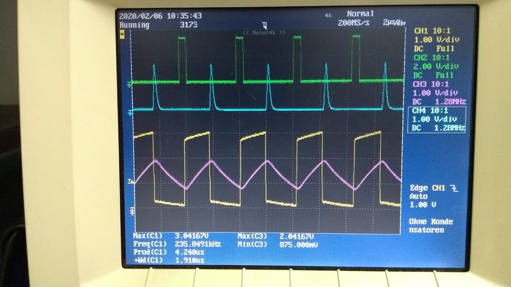
Here are the waveforms:
Green is COMP1 output
Blue is COMP2 output
Yellow is PWM H output (is driving a RC to generate the test signal)
Purple is the test signal being injected into both comparators inputs (PA1)
I set all polarities in the break configuration to active HIGH, and configured the COMP1 (green, ETR source for timer reset) as inverted (it goes HIGH when the signal is lower than the DAC setting)
Here is my timer initialization code, generated with CubeMX:
void MX_TIM1_Init(void)
{
  LL_TIM_InitTypeDef TIM_InitStruct = {0};
  LL_TIM_OC_InitTypeDef TIM_OC_InitStruct = {0};
  LL_TIM_BDTR_InitTypeDef TIM_BDTRInitStruct = {0};

  LL_GPIO_InitTypeDef GPIO_InitStruct = {0};
  /* Peripheral clock enable */
  LL_APB2_GRP1_EnableClock(LL_APB2_GRP1_PERIPH_TIM1);

  TIM_InitStruct.Prescaler = 0;
  TIM_InitStruct.CounterMode = LL_TIM_COUNTERMODE_UP;
  TIM_InitStruct.Autoreload = 65535;
  TIM_InitStruct.ClockDivision = LL_TIM_CLOCKDIVISION_DIV1;
  TIM_InitStruct.RepetitionCounter = 0;
  LL_TIM_Init(TIM1, &TIM_InitStruct);
  LL_TIM_DisableARRPreload(TIM1);
  LL_TIM_SetClockSource(TIM1, LL_TIM_CLOCKSOURCE_INTERNAL);
  LL_TIM_OC_EnablePreload(TIM1, LL_TIM_CHANNEL_CH1);
  TIM_OC_InitStruct.OCMode = LL_TIM_OCMODE_PWM1;
  TIM_OC_InitStruct.OCState = LL_TIM_OCSTATE_DISABLE;
  TIM_OC_InitStruct.OCNState = LL_TIM_OCSTATE_DISABLE;
  TIM_OC_InitStruct.CompareValue = 32768;
  TIM_OC_InitStruct.OCPolarity = LL_TIM_OCPOLARITY_HIGH;
  TIM_OC_InitStruct.OCNPolarity = LL_TIM_OCPOLARITY_HIGH;
  TIM_OC_InitStruct.OCIdleState = LL_TIM_OCIDLESTATE_LOW;
  TIM_OC_InitStruct.OCNIdleState = LL_TIM_OCIDLESTATE_HIGH;
  LL_TIM_OC_Init(TIM1, LL_TIM_CHANNEL_CH1, &TIM_OC_InitStruct);
  LL_TIM_OC_DisableFast(TIM1, LL_TIM_CHANNEL_CH1);
  LL_TIM_SetTriggerInput(TIM1, LL_TIM_TS_ETRF);
  LL_TIM_SetSlaveMode(TIM1, LL_TIM_SLAVEMODE_RESET);
  LL_TIM_DisableExternalClock(TIM1);
  LL_TIM_ConfigETR(TIM1, LL_TIM_ETR_POLARITY_NONINVERTED, LL_TIM_ETR_PRESCALER_DIV1, LL_TIM_ETR_FILTER_FDIV1);
  LL_TIM_DisableIT_TRIG(TIM1);
  LL_TIM_DisableDMAReq_TRIG(TIM1);
  LL_TIM_SetTriggerOutput(TIM1, LL_TIM_TRGO_RESET);
  LL_TIM_SetTriggerOutput2(TIM1, LL_TIM_TRGO2_RESET);
  LL_TIM_DisableMasterSlaveMode(TIM1);
  LL_TIM_SetBreakInputSourcePolarity(TIM1, LL_TIM_BREAK_INPUT_BKIN, LL_TIM_BKIN_SOURCE_BKCOMP2, ((uint32_t)0x00000000U));
  LL_TIM_SetETRSource(TIM1, LL_TIM_ETRSOURCE_COMP1);
  LL_TIM_OC_DisablePreload(TIM1, LL_TIM_CHANNEL_CH1);
  TIM_BDTRInitStruct.OSSRState = LL_TIM_OSSR_DISABLE;
  TIM_BDTRInitStruct.OSSIState = LL_TIM_OSSI_ENABLE;
  TIM_BDTRInitStruct.LockLevel = LL_TIM_LOCKLEVEL_OFF;
  TIM_BDTRInitStruct.DeadTime = 32;
  TIM_BDTRInitStruct.BreakState = LL_TIM_BREAK_ENABLE;
  TIM_BDTRInitStruct.BreakPolarity = LL_TIM_BREAK_POLARITY_HIGH;
  TIM_BDTRInitStruct.BreakFilter = LL_TIM_BREAK_FILTER_FDIV1;
  TIM_BDTRInitStruct.BreakAFMode = LL_TIM_BREAK_AFMODE_INPUT;
  TIM_BDTRInitStruct.Break2State = LL_TIM_BREAK2_DISABLE;
  TIM_BDTRInitStruct.Break2Polarity = LL_TIM_BREAK2_POLARITY_HIGH;
  TIM_BDTRInitStruct.Break2Filter = LL_TIM_BREAK2_FILTER_FDIV1;
  TIM_BDTRInitStruct.Break2AFMode = LL_TIM_BREAK_AFMODE_INPUT;
  TIM_BDTRInitStruct.AutomaticOutput = LL_TIM_AUTOMATICOUTPUT_ENABLE;
  LL_TIM_BDTR_Init(TIM1, &TIM_BDTRInitStruct);
  LL_IOP_GRP1_EnableClock(LL_IOP_GRP1_PERIPH_GPIOA);
    /**TIM1 GPIO Configuration
    PA7     ------> TIM1_CH1N
    PA8     ------> TIM1_CH1
    */
  GPIO_InitStruct.Pin = LL_GPIO_PIN_7;
  GPIO_InitStruct.Mode = LL_GPIO_MODE_ALTERNATE;
  GPIO_InitStruct.Speed = LL_GPIO_SPEED_FREQ_HIGH;
  GPIO_InitStruct.OutputType = LL_GPIO_OUTPUT_PUSHPULL;
  GPIO_InitStruct.Pull = LL_GPIO_PULL_NO;
  GPIO_InitStruct.Alternate = LL_GPIO_AF_2;
  LL_GPIO_Init(GPIOA, &GPIO_InitStruct);

  GPIO_InitStruct.Pin = LL_GPIO_PIN_8;
  GPIO_InitStruct.Mode = LL_GPIO_MODE_ALTERNATE;
  GPIO_InitStruct.Speed = LL_GPIO_SPEED_FREQ_HIGH;
  GPIO_InitStruct.OutputType = LL_GPIO_OUTPUT_PUSHPULL;
  GPIO_InitStruct.Pull = LL_GPIO_PULL_NO;
  GPIO_InitStruct.Alternate = LL_GPIO_AF_2;
  LL_GPIO_Init(GPIOA, &GPIO_InitStruct);

}
And here is the main code, which starts everything:
  MX_COMP1_Init();
  MX_COMP2_Init();
  MX_DAC1_Init();
  MX_TIM1_Init();

  HAL_DAC_Start(&hdac1,DAC_CHANNEL_1);
  HAL_DAC_Start(&hdac1,DAC_CHANNEL_2);

  HAL_DAC_SetValue(&hdac1,DAC_CHANNEL_1,DAC_ALIGN_8B_R,77); // 1V
  HAL_DAC_SetValue(&hdac1,DAC_CHANNEL_2,DAC_ALIGN_8B_R,154); // 2V

  HAL_COMP_Start(&hcomp1);
  HAL_COMP_Start(&hcomp2);

  //LL_TIM_OC_SetCompareCH1(TIM1,5000);
  //LL_TIM_SetAutoReload(TIM1,40000);

  LL_TIM_CC_EnableChannel(TIM1, LL_TIM_CHANNEL_CH1|LL_TIM_CHANNEL_CH1N);
  LL_TIM_EnableBreakInputSource(TIM1,LL_TIM_BREAK_INPUT_BKIN,LL_TIM_BKIN_SOURCE_BKCOMP2);
  LL_TIM_EnableAllOutputs(TIM1);
LL_TIM_EnableCounter(TIM1);- Mark as New
- Bookmark
- Subscribe
- Mute
- Subscribe to RSS Feed
- Permalink
- Email to a Friend
- Report Inappropriate Content
2020-02-06 12:53 AM
I don't understand the Cube gobbledygook.
Please read out and post content of TIM1 and the COMP-related registers.
JW
- Mark as New
- Bookmark
- Subscribe
- Mute
- Subscribe to RSS Feed
- Permalink
- Email to a Friend
- Report Inappropriate Content
2020-02-06 2:36 AM
Alright, here are the values right after everything is set:
TIM1	TIM_TypeDef *	0x40012c00 (Hex)
	CR1	volatile uint32_t	0x1 (Hex)
	CR2	volatile uint32_t	0x200 (Hex)
	SMCR	volatile uint32_t	0x74 (Hex)
	DIER	volatile uint32_t	0x0 (Hex)
	SR	volatile uint32_t	0x300dd (Hex)
	EGR	volatile uint32_t	0x0 (Hex)
	CCMR1	volatile uint32_t	0x60 (Hex)
	CCMR2	volatile uint32_t	0x0 (Hex)
	CCER	volatile uint32_t	0x5 (Hex)
	CNT	volatile uint32_t	0x5c (Hex)
	PSC	volatile uint32_t	0x0 (Hex)
	ARR	volatile uint32_t	0xffff (Hex)
	RCR	volatile uint32_t	0x0 (Hex)
	CCR1	volatile uint32_t	0x8000 (Hex)
	CCR2	volatile uint32_t	0x0 (Hex)
	CCR3	volatile uint32_t	0x0 (Hex)
	CCR4	volatile uint32_t	0x0 (Hex)
	BDTR	volatile uint32_t	0x2007420 (Hex)
	DCR	volatile uint32_t	0x0 (Hex)
	DMAR	volatile uint32_t	0x1 (Hex)
	OR1	volatile uint32_t	0x0 (Hex)
	CCMR3	volatile uint32_t	0x0 (Hex)
	CCR5	volatile uint32_t	0x0 (Hex)
	CCR6	volatile uint32_t	0x0 (Hex)
	AF1	volatile uint32_t	0x4005 (Hex)
	AF2	volatile uint32_t	0x1 (Hex)
	TISEL	volatile uint32_t	0x0 (Hex)
COMP1	COMP_TypeDef *	0x40010200 (Hex)
	CSR	volatile uint32_t	0x38241 (Hex)
COMP2	COMP_TypeDef *	0x40010204 (Hex)
CSR volatile uint32_t 0x30851 (Hex) - Mark as New
- Bookmark
- Subscribe
- Mute
- Subscribe to RSS Feed
- Permalink
- Email to a Friend
- Report Inappropriate Content
2020-02-06 9:58 AM
Get rid of all BREAK-related stuff, don't use BREAK nor BREAK2.
Try (with long pulse in timer), report back (together with waveforms and the registers content).
JW
- Mark as New
- Bookmark
- Subscribe
- Mute
- Subscribe to RSS Feed
- Permalink
- Email to a Friend
- Report Inappropriate Content
2020-02-06 11:59 PM
Hi Jan!
Here it is, the timer is configured to run @128MHz
Register content:
TIM1	TIM_TypeDef *	0x40012c00 (Hex)
	CR1	volatile uint32_t	0x1 (Hex)
	CR2	volatile uint32_t	0x200 (Hex)
	SMCR	volatile uint32_t	0x74 (Hex)
	DIER	volatile uint32_t	0x0 (Hex)
	SR	volatile uint32_t	0x3005f (Hex)
	EGR	volatile uint32_t	0x0 (Hex)
	CCMR1	volatile uint32_t	0xe0 (Hex)
	CCMR2	volatile uint32_t	0x0 (Hex)
	CCER	volatile uint32_t	0x5 (Hex)
	CNT	volatile uint32_t	0x1aaf (Hex)
	PSC	volatile uint32_t	0x0 (Hex)
	ARR	volatile uint32_t	0xffff (Hex)
	RCR	volatile uint32_t	0x0 (Hex)
	CCR1	volatile uint32_t	0x1400 (Hex)
	CCR2	volatile uint32_t	0x0 (Hex)
	CCR3	volatile uint32_t	0x0 (Hex)
	CCR4	volatile uint32_t	0x0 (Hex)
	BDTR	volatile uint32_t	0x200a420 (Hex)
	DCR	volatile uint32_t	0x0 (Hex)
	DMAR	volatile uint32_t	0x1 (Hex)
	OR1	volatile uint32_t	0x1 (Hex)
	CCMR3	volatile uint32_t	0x0 (Hex)
	CCR5	volatile uint32_t	0x0 (Hex)
	CCR6	volatile uint32_t	0x0 (Hex)
	AF1	volatile uint32_t	0x4001 (Hex)
	AF2	volatile uint32_t	0x1 (Hex)
	TISEL	volatile uint32_t	0x0 (Hex)
COMP1	COMP_TypeDef *	0x40010200 (Hex)
	CSR	volatile uint32_t	0x38241 (Hex)
COMP2	COMP_TypeDef *	0x40010204 (Hex)
	CSR	volatile uint32_t	0x30851 (Hex)
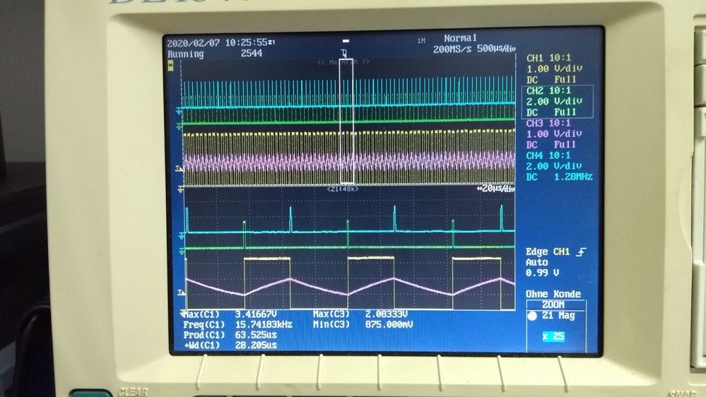
Waveform with CCR1 = 0x1400 (40us, register content above), it works:
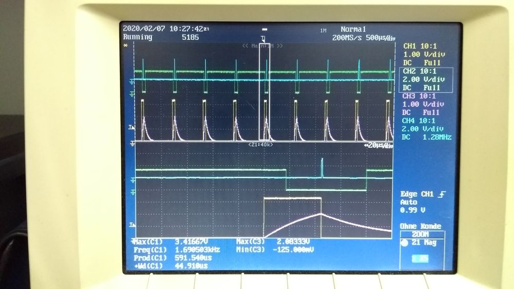
Yellow is the PWM output
Purple is the signal being fed to both comparators
Green is COMP1 output
Blue is COMP2 output
With the same configuration, but with CCR1 = 0x3200 (100us), it stop working the slave reset, and the maximum period (ARR = 0xFFFF, 512us) happens:
Do you have any idea why the Slave reset does not work only when OCREF_CLR is used and the CCR period is still "on" ?
Thanks again
Gustavo
- Mark as New
- Bookmark
- Subscribe
- Mute
- Subscribe to RSS Feed
- Permalink
- Email to a Friend
- Report Inappropriate Content
2020-02-07 2:32 AM
Hi Gustavo,
it looks that you've tapped into a genuine hardware bug.
Can you please, for the non-working case
- measure exactly the period - IMO it's not 512us but (80+512)us - 80us being the time beteen previous reset and COMP1 rising edge (where reset does occur but errorneously does not set OC1REF)
- output on an unrelated channel's pin (e.g. CH2) a PWM with short CCRx setting and measure it together with the above waveforms
@Vincent Onde ,
Can you please have a look at this problem? It appears, that when OCREF_CLR clears OC1REF, and Update event happens (here through slave-mode controller's Reset) *before* CNT>CCR1, OC1REF does not get set properly at Update again.
Thanks,
Jan
- Interfacing STM Nucleo F767ZI White Board with W25Q256JV using QSPI in STM32 MCUs Products
- STM32CubeIDE_1.17.0 crash after few seconds in STM32CubeIDE (MCUs)
- Input capture / Frequency Measurement error on STM32U545REQ in STM32 MCUs Products
- Using integrated DB function of STM32U5 with TCPP01-M12 in STM32 MCUs Products
- Implementing STM32L4S5ZIT6 Bootloader with a Memory Marker in STM32 MCUs Products


