- STMicroelectronics Community
- STM32 MCUs
- STM32 MCUs products
- How to change the clock frequency on a STM32H753ZI
- Subscribe to RSS Feed
- Mark Topic as New
- Mark Topic as Read
- Float this Topic for Current User
- Bookmark
- Subscribe
- Mute
- Printer Friendly Page
How to change the clock frequency on a STM32H753ZI
- Mark as New
- Bookmark
- Subscribe
- Mute
- Subscribe to RSS Feed
- Permalink
- Email to a Friend
- Report Inappropriate Content
2020-09-29 08:59 PM
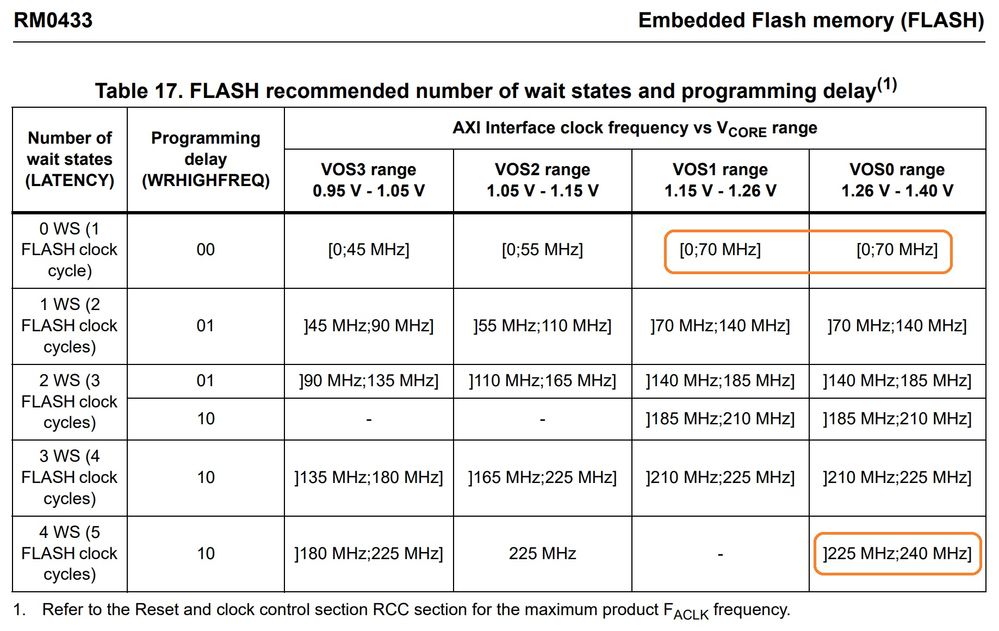
Hey guys completely lost on this one. I have seen many other STM32 chipsets and in the reference manual its plain and simple how to increase it, however when it comes to this chip it doesnt list the Wait state for the CPU frequency but for the AXI peripherals?
Any ideas how to change the clock frequency for this chip particular?
Referring to Table 17 in the reference sheet
- Labels:
-
Flash
-
STM32H7 Series
- Mark as New
- Bookmark
- Subscribe
- Mute
- Subscribe to RSS Feed
- Permalink
- Email to a Friend
- Report Inappropriate Content
2020-09-29 09:31 PM
The primary takeaway is that the AXIM while 64-bit wide clocks at half the core speed. The dual-ported FLASH is attached to the AXIM, and the wait states on the memory lines is based on the 200 to 240 MHz clock, and the power settings (higher voltage, faster memory).
One wait-state per 60-70 MHz, typically 4 WS for the CPU clocking at maximum
The only memory running at 400/480 MHz is the Cache and TCM, the bus width of the AXIM yielding similar bandwidth, but higher latency.
Up vote any posts that you find helpful, it shows what's working..
- Mark as New
- Bookmark
- Subscribe
- Mute
- Subscribe to RSS Feed
- Permalink
- Email to a Friend
- Report Inappropriate Content
2020-09-29 09:55 PM
Thanks for the quick answer, however I have more questions.
- How do you know the AXIM clocks at half of the core speed.
- How did you get the One wait state per 60-70MHz
- Why isnt this documented in the reference Manuel?
- Mark as New
- Bookmark
- Subscribe
- Mute
- Subscribe to RSS Feed
- Permalink
- Email to a Friend
- Report Inappropriate Content
2020-09-29 10:46 PM
The documentation is weak when it comes to the clocking, but there is plenty of data in the materials when judged as a whole.
70/1 = 70
140/2 = 70
185/3 = 61.6667
210/3 = 70
225/4 = 56.25
240/5 = 48
The last two are very conservative, a core running north of 500 MHZ doesn't run out of head room. The H7 was designed as a multi-core system, there are models rated to 550 MHz
1) it is an inference based on the maximal speed of everything attached to it, definitely not higher than 300 MHz, and FMC on at least one board can't exceed 200 MHz based on the memory attached externally.
The AHB bus routes straight thru the switching fabric, sharing a common domain. The APBs run off the AHB
/**
* @brief System Clock Configuration
* The system Clock is configured as follow :
* System Clock source = PLL (HSE BYPASS)
* SYSCLK(Hz) = 400000000 (CPU Clock)
* HCLK(Hz) = 200000000 (AXI and AHBs Clock)
* AHB Prescaler = 2
* D1 APB3 Prescaler = 2 (APB3 Clock 100MHz)
* D2 APB1 Prescaler = 2 (APB1 Clock 100MHz)
* D2 APB2 Prescaler = 2 (APB2 Clock 100MHz)
* D3 APB4 Prescaler = 2 (APB4 Clock 100MHz)
* HSE Frequency(Hz) = 8000000
* PLL_M = 4
* PLL_N = 400
* PLL_P = 2
* PLL_Q = 4
* PLL_R = 2
* VDD(V) = 3.3
* Flash Latency(WS) = 4
* @param None
* @retval None
*/
Up vote any posts that you find helpful, it shows what's working..
- Mark as New
- Bookmark
- Subscribe
- Mute
- Subscribe to RSS Feed
- Permalink
- Email to a Friend
- Report Inappropriate Content
2020-09-29 11:19 PM
so would you take the average of all those Clocks? So ~ 5 WS should get you to 480MHz?
- Mark as New
- Bookmark
- Subscribe
- Mute
- Subscribe to RSS Feed
- Permalink
- Email to a Friend
- Report Inappropriate Content
2020-09-29 11:29 PM
4 WS would be 5 cycles total for the transaction on the 240 MHz bus.
The CM7 would be clocking at 480 MHz.
Up vote any posts that you find helpful, it shows what's working..
- Mark as New
- Bookmark
- Subscribe
- Mute
- Subscribe to RSS Feed
- Permalink
- Email to a Friend
- Report Inappropriate Content
2020-09-30 12:12 AM
fair enough. If you know the AXIM peripherals are half the clock speed then why do that math there?
- ST-Link-V3 on MacBook Pro M2 running Sonoma 14.4 only works through hub in STM32 MCUs Boards and hardware tools
- PWM behavior when changing deadtime during operation in STM32 MCUs Motor control
- Triangle wave DAC output on STM32G473 seems to be stuck enabled on all channels in STM32 MCUs products
- Power Regulator Voltage scaling and SysClock issue in STM32CubeIDE (MCUs)
- STM32CubeProgrammer 2.16.0 released in STM32CubeProgrammer (MCUs)
