- STMicroelectronics Community
- STM32 MCUs Software development tools
- STM32CubeMX (MCUs)
- STM32F769I-DISC1 only 64Mb accessible?
- Subscribe to RSS Feed
- Mark Topic as New
- Mark Topic as Read
- Float this Topic for Current User
- Bookmark
- Subscribe
- Mute
- Printer Friendly Page
STM32F769I-DISC1 only 64Mb accessible?
- Mark as New
- Bookmark
- Subscribe
- Mute
- Subscribe to RSS Feed
- Permalink
- Email to a Friend
- Report Inappropriate Content
2020-07-19 08:47 AM
Hi everyone!
I'm new to the forum so please let me know if I should add more information, etc..
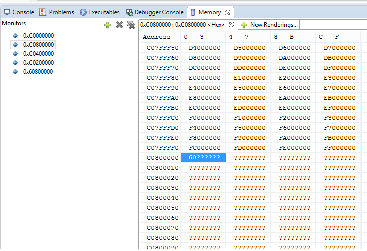
I am using the external SDRAM (MT48LC4M32B2B5-6A, 128Mb) on the STM32F769I-DISC1 board. The SDRAM was configured with CubeMX to use all four memory banks. Everything works fine if I access memory regions from 0xC0000000 to 0xC0800000 (corresponding to 64Mb). If I try to access memory locations beyond 0xC0800000 the MCU ends up in the Hardfault handler.
Has someone else experienced this issue?
What is the easiest way to check if the SDRAM was correctly set up to use 4 memory banks?
Thanks for your help!
Solved! Go to Solution.
- Labels:
-
STM32CubeMX
-
STM32F7 Series
Accepted Solutions
- Mark as New
- Bookmark
- Subscribe
- Mute
- Subscribe to RSS Feed
- Permalink
- Email to a Friend
- Report Inappropriate Content
2020-07-20 01:23 AM
Sorry for wasting your time, the problem was indeed with the 16 bit values, if I write 32 bit values I can use all 128Mb.
So in order to write 128Mb of 16 bit values I will need to use a bus width of 32 and pack two 16 bit values into one 32 bit variable that can then be written to the SDRAM?
- Mark as New
- Bookmark
- Subscribe
- Mute
- Subscribe to RSS Feed
- Permalink
- Email to a Friend
- Report Inappropriate Content
2020-07-19 08:56 AM
As I recall they only wired half the data pins, to save pins, while getting a part footprint and price that suited them.
Up vote any posts that you find helpful, it shows what's working..
- Mark as New
- Bookmark
- Subscribe
- Mute
- Subscribe to RSS Feed
- Permalink
- Email to a Friend
- Report Inappropriate Content
2020-07-19 09:06 AM
Thanks for your answer clive1!
That's the first thing I checked and it seems that with other boards that have only half the pins wired up it says "128Mb (64Mb accessible)" in the board description, which is not the case for the STM32F769I-DISC1. Also, when checking the schematic for the discovery board it looks like all 32 data pins are actually wired to the MCU.
I don't know if there could be a difference between STM32F769I-DISC1 and STM32F769I-DISC0 (the latter having all 32 data pins wired while the first one doesn't) but there is only one documentation as far as I can tell.
- Mark as New
- Bookmark
- Subscribe
- Mute
- Subscribe to RSS Feed
- Permalink
- Email to a Friend
- Report Inappropriate Content
2020-07-19 10:52 AM
Working from memory.
So if it hard faults need to review programmed geometry. Banks, address lines (row, columns), banks and bus width.
Up vote any posts that you find helpful, it shows what's working..
- Mark as New
- Bookmark
- Subscribe
- Mute
- Subscribe to RSS Feed
- Permalink
- Email to a Friend
- Report Inappropriate Content
2020-07-19 10:52 AM
DISCO vs DISC1 is the screen, or not
Up vote any posts that you find helpful, it shows what's working..
- Mark as New
- Bookmark
- Subscribe
- Mute
- Subscribe to RSS Feed
- Permalink
- Email to a Friend
- Report Inappropriate Content
2020-07-19 11:03 AM
/* FMC initialization function */
static void MX_FMC_Init(void)
{
  FMC_SDRAM_TimingTypeDef SdramTiming = {0};

  /** Perform the SDRAM1 memory initialization sequence */
  hsdram1.Instance = FMC_SDRAM_DEVICE;
  /* hsdram1.Init */
  hsdram1.Init.SDBank = FMC_SDRAM_BANK1;
  hsdram1.Init.ColumnBitsNumber = FMC_SDRAM_COLUMN_BITS_NUM_8;
  hsdram1.Init.RowBitsNumber = FMC_SDRAM_ROW_BITS_NUM_12;
  hsdram1.Init.MemoryDataWidth = FMC_SDRAM_MEM_BUS_WIDTH_16;
  hsdram1.Init.InternalBankNumber = FMC_SDRAM_INTERN_BANKS_NUM_4;
  hsdram1.Init.CASLatency = FMC_SDRAM_CAS_LATENCY_2;
  hsdram1.Init.WriteProtection = FMC_SDRAM_WRITE_PROTECTION_DISABLE;
  hsdram1.Init.SDClockPeriod = FMC_SDRAM_CLOCK_PERIOD_2;
  hsdram1.Init.ReadBurst = FMC_SDRAM_RBURST_DISABLE;
  hsdram1.Init.ReadPipeDelay = FMC_SDRAM_RPIPE_DELAY_0;
  /* SdramTiming */
  SdramTiming.LoadToActiveDelay = 2;
  SdramTiming.ExitSelfRefreshDelay = 6;
  SdramTiming.SelfRefreshTime = 4;
  SdramTiming.RowCycleDelay = 6;
  SdramTiming.WriteRecoveryTime = 2;
  SdramTiming.RPDelay = 2;
  SdramTiming.RCDDelay = 2;

  if (HAL_SDRAM_Init(&hsdram1, &SdramTiming) != HAL_OK)
  {
    Error_Handler( );
  }
}
This is the initialization of the FMC.
Could the problem have anything to do with the fact that I am trying to write 16 bit data?
I thought the FMC is supposed to present the SDRAM memory as a continuous memory region to the programmer, so I shouldn't have to worry about writing 8 bit, 16 bit or 32 bit values.
Or can the full memory only be used with a bus width of 32 because these are the only physical connections available to this memory regions?
- Mark as New
- Bookmark
- Subscribe
- Mute
- Subscribe to RSS Feed
- Permalink
- Email to a Friend
- Report Inappropriate Content
2020-07-20 01:23 AM
Sorry for wasting your time, the problem was indeed with the 16 bit values, if I write 32 bit values I can use all 128Mb.
So in order to write 128Mb of 16 bit values I will need to use a bus width of 32 and pack two 16 bit values into one 32 bit variable that can then be written to the SDRAM?
- Mark as New
- Bookmark
- Subscribe
- Mute
- Subscribe to RSS Feed
- Permalink
- Email to a Friend
- Report Inappropriate Content
2020-11-07 01:56 PM
Hi!
I'm facing the same problem with the memory access above 0xC080 0000:
The difference is, that I'm already using a 32bit variables to write and read from the SDRAM.
uint32_t RxBuffer[SDRAM_TEST_BUFFER_SIZE], TxBuffer[SDRAM_TEST_BUFFER_SIZE];Do you have any hints what I can still check?
Regards,
Gregor
- Mark as New
- Bookmark
- Subscribe
- Mute
- Subscribe to RSS Feed
- Permalink
- Email to a Friend
- Report Inappropriate Content
2020-11-08 01:57 AM
Hi Gregor!
Your configuration looks correct, does everything work as expected if you fill up the SDRAM up to 0xC080 0000?
Is everything behaving identical if you configure the SDRAM to only use 2 memory banks? Is there a way you can check if the pin for configuring the 4 memory banks is actually set?
Regards
- Mark as New
- Bookmark
- Subscribe
- Mute
- Subscribe to RSS Feed
- Permalink
- Email to a Friend
- Report Inappropriate Content
2020-11-08 03:10 AM
Hi FGeig.1 !
Yes, when I write data into the SDRAM, read out and compare, then I get a 1:1 match.
After attempt to write above 0xC080 0000 I get a HW fault.
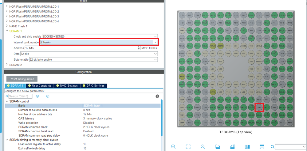
Now I have tried to reduce the configuration to 2 banks and the result is the same:

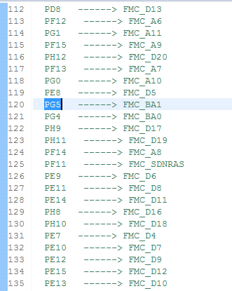
When do this, then the BA1 pin (PG5) is deconfigured in the pin overview:

In the configuration of the fmc.c I can see the bank pins:
  /* GPIO_InitStruct */
  GPIO_InitStruct.Pin = GPIO_PIN_15|GPIO_PIN_8|GPIO_PIN_1|GPIO_PIN_0
                          |GPIO_PIN_5|GPIO_PIN_4;
  GPIO_InitStruct.Mode = GPIO_MODE_AF_PP;
  GPIO_InitStruct.Pull = GPIO_NOPULL;
  GPIO_InitStruct.Speed = GPIO_SPEED_FREQ_VERY_HIGH;
  GPIO_InitStruct.Alternate = GPIO_AF12_FMC;

  HAL_GPIO_Init(GPIOG, &GPIO_InitStruct);
However in the STM32F767NIHX_RAM.ld file I can't see any SDRAM section:
/* Entry Point */
ENTRY(Reset_Handler)

/* Highest address of the user mode stack */
_estack = ORIGIN(RAM) + LENGTH(RAM);	/* end of "RAM" Ram type memory */

_Min_Heap_Size = 0x200;	/* required amount of heap  */
_Min_Stack_Size = 0x400;	/* required amount of stack */

/* Memories definition */
MEMORY
{
  RAM    (xrw)    : ORIGIN = 0x20000000,   LENGTH = 512K
  FLASH    (rx)    : ORIGIN = 0x8000000,   LENGTH = 2048K
}
Is this ok? How the controller is allocating the memory and where?
Regards,
Gregor
- STM32H5xx - CUBE MX 6.13 - Error activating RTC Clock source for Backup register access in STM32CubeMX (MCUs)
- Accessing FDCAN System bootloader with STLINK/V3 + CubeProgrammer in STM32CubeProgrammer (MCUs)
- Unable to access Calibration Words with STM32H503RBT in STM32CubeIDE (MCUs)
- stm32cubemx failed to open ACCESS TO MCU SELECTOR in STM32CubeMX (MCUs)
- STM32H757I-EVAL / Issue of NDTR Access with UART and DMA in STM32CubeIDE (MCUs)
