- STMicroelectronics Community
- STM32 MCUs Software development tools
- STM32CubeIDE (MCUs)
- Re: How to use STM32CubeIDE or STM32CubeMX to auto...
- Subscribe to RSS Feed
- Mark Topic as New
- Mark Topic as Read
- Float this Topic for Current User
- Bookmark
- Subscribe
- Mute
- Printer Friendly Page
How to use STM32CubeIDE or STM32CubeMX to automatically add settings for RAM_D2 and RAM_D3 in LD fil
- Mark as New
- Bookmark
- Subscribe
- Mute
- Subscribe to RSS Feed
- Permalink
- Email to a Friend
- Report Inappropriate Content
2024-02-09 07:58 PM - edited 2024-02-09 08:00 PM
Hi All,
Requesting help with below.
I am using latest version of STM32CubeIDE. The microcontroller in use is STM32H743BITx.
I have concerns with regards to:
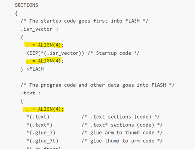
1. Whether to add ALIGN(4) even inside the FLASH sections present in STM32H753BITX_FLASH.ld (attached)
2. The file generated by STM32CubeMX (ran from within STM32CubeIDE) generated a STM32H753BITX_FLASH.ld file in the project folder. It does not contain sections that reside in RAM_D2 and RAM_D3. Attached the STM32H753BITX_FLASH.ld.txt file for reference. Is there a way available with STM32CubeMX (preferably) or with STM32CubeIDE to add the necessary RAM sections in the LD file for STM32H743BITx?
3. I observe that macro DATA_IN_D2_SRAM is disabled and hence concerned about how clocks to RAM_D1, RAM_D2 and RAM_D3 are being enabled. I am also unable to figure out any valid assignment to register AHB2ENR which would enable the clock to the three RAM sections.
In file system_stm32h7xx.c please refer to below section starting at line number 79.
The macro DATA_IN_D2_SRAM is disabled
/************************* Miscellaneous Configuration ************************/
/*!< Uncomment the following line if you need to use initialized data in D2 domain SRAM (AHB SRAM) */
/* #define DATA_IN_D2_SRAM */
Then from line number 267
#if defined(DATA_IN_D2_SRAM)
/* in case of initialized data in D2 SRAM (AHB SRAM), enable the D2 SRAM clock (AHB SRAM clock) */
#if defined(RCC_AHB2ENR_D2SRAM3EN)
RCC->AHB2ENR |= (RCC_AHB2ENR_D2SRAM1EN | RCC_AHB2ENR_D2SRAM2EN | RCC_AHB2ENR_D2SRAM3EN);
#elif defined(RCC_AHB2ENR_D2SRAM2EN)
RCC->AHB2ENR |= (RCC_AHB2ENR_D2SRAM1EN | RCC_AHB2ENR_D2SRAM2EN);
#else
RCC->AHB2ENR |= (RCC_AHB2ENR_AHBSRAM1EN | RCC_AHB2ENR_AHBSRAM2EN);
#endif /* RCC_AHB2ENR_D2SRAM3EN */
tmpreg = RCC->AHB2ENR;
(void) tmpreg;
#endif /* DATA_IN_D2_SRAM */
Please help resolve my above concerns.
Thanks!
Rajeev
Solved! Go to Solution.
- Labels:
-
STM32CubeIDE
-
STM32CubeMX
Accepted Solutions
- Mark as New
- Bookmark
- Subscribe
- Mute
- Subscribe to RSS Feed
- Permalink
- Email to a Friend
- Report Inappropriate Content
2024-02-11 08:30 PM - edited 2024-02-11 11:18 PM
Additional response:
I believe there are two modifications/options and that I should add/enable one.
As you suggested I can either add code to file startup_stm32h753bitx.s (the one present on the right is the update):
Or alternately enable the macro DATA_IN_D2_SRAM present in file system_stm32h7xx.c (the one present on the right is the update):
I shall first try with updating the Code in above C file. If it does not work, then only I'll add the code to the above .S file.
Previous response:
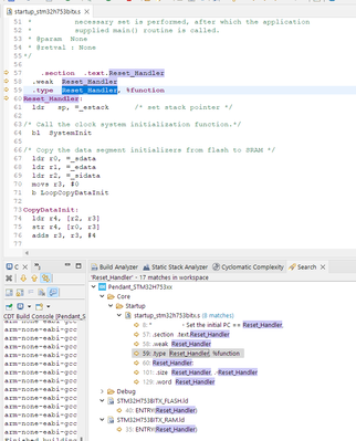
I am compiling code using STM32CubeIDE and the code was generated using STM32CubeMX.
I only find below references for Reset_Handler. I do not find the line number 7 that is present in the snippet you shared. Which file should I look for the code snippet that you have shared?
- Mark as New
- Bookmark
- Subscribe
- Mute
- Subscribe to RSS Feed
- Permalink
- Email to a Friend
- Report Inappropriate Content
2024-02-10 06:48 AM
CubeMX only provides those premade linker scripts. If you want something different, you need to edit the file yourself and add/change the sections.
- Mark as New
- Bookmark
- Subscribe
- Mute
- Subscribe to RSS Feed
- Permalink
- Email to a Friend
- Report Inappropriate Content
2024-02-10 11:50 AM - edited 2024-02-10 11:50 AM
Hi,
1 > Whether to add ALIGN(4) even inside the FLASH sections present ..
yes, in all sections.
2 > .. as TDK told : you have to set, what you want.
3> I dont know , what you ask about, i just set the sections as i want and it works. (on H743 )
- Mark as New
- Bookmark
- Subscribe
- Mute
- Subscribe to RSS Feed
- Permalink
- Email to a Friend
- Report Inappropriate Content
2024-02-11 09:49 AM
Hi @Khouloud ZEMMELI , @AScha.3
Since answer to my first query is Yes, I believe the default STM32H753BITX_FLASH.ld file provided/added by ST should be updated to include the ALIGN(4) in all sections (especially in the FLASH sections). I would request ST / Khouloud (and her team) to update STM32CubeIDE so that the updated file is available when user generates the code.
@AScha.3I would like to understand from you about whether any of your firmware uses the RAM which is being refereed to as RAM_D2, and RAM_D3
Below is what could be added to MEMORY section:
RAM_D1 (xrw) : ORIGIN = 0x24000000, LENGTH = 512K /* AXI SRAM section */
RAM_D2 (xrw) : ORIGIN = 0x30000000, LENGTH = 288K /* SRAM 1 + SRAM 2 + SRAM 3 */
RAM_D3 (xrw) : ORIGIN = 0x38000000, LENGTH = 64K /* SRAM 4 */
Later similar to how various RAM sections are defined (with the closing brackets being followed by ">RAM_D1" (but without quotes)) what sections do I declare using RAM_D2 and RAM_D3. And how do I ensure that RAM_D3 gets filled before RAM_D2, and RAM_D2 gets filled before RAM_D1.
In SCT file (linker file) which was used by Keil IDE we used the keyword .ANY followed by a number (The higher the number, the higher the priority of the section being used by variables).
Please share your inputs.
Regards,
Rajeev
- Mark as New
- Bookmark
- Subscribe
- Mute
- Subscribe to RSS Feed
- Permalink
- Email to a Friend
- Report Inappropriate Content
2024-02-11 09:59 AM
> I believe the default STM32H753BITX_FLASH.ld file provided/added by ST should be updated to include the ALIGN(4) in all sections (especially in the FLASH sections).
The linker script already has alignment to 32-bit words.
> And how do I ensure that RAM_D3 gets filled before RAM_D2, and RAM_D2 gets filled before RAM_D1.
Assignments to a particular section must be done explicitly. The linker can not split them up based on available space. To specify a section, use the attribute in the variable definition. Here is a link for how to do that:
- Mark as New
- Bookmark
- Subscribe
- Mute
- Subscribe to RSS Feed
- Permalink
- Email to a Friend
- Report Inappropriate Content
2024-02-11 10:04 AM
Thanks @TDK for a quick response.
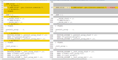
I observe below when comparing the file that my team uses (on left) and the one that STM32CubeMX generated (on the right):
Regards,
Rajeev
- Mark as New
- Bookmark
- Subscribe
- Mute
- Subscribe to RSS Feed
- Permalink
- Email to a Friend
- Report Inappropriate Content
2024-02-11 10:14 AM
Hi @TDK
From your second input I understand that while declaring any variable, I'll have to ensure that it is preceded with the __attribute__ and the section() keywords, along with the section name.
Below is part of my SCT file that I use with Keil compiler. If I want to create a LD file with similar data, then this is not possible, as there is no keyword with LD file which equals/is-similar to the the ANY keyword being used.
Is my above understanding correct?
;**** PART OF SCT FILE START *****
RW_RAM1 0x30000000 0x00020000 { ; RW data
.ANY (+RW +ZI)
}
RW_RAM2 0x30020000 0x00020000 {
.ANY (+RW +ZI)
}
RW_RAM3 0x30040000 0x00008000 { ; should be used for creating buffers for ETHERNET and USB
.ANY (+RW +ZI)
}
RW_IRAM1 0x20000000 0x00020000 { ; RW data
.ANY99 (+RW +ZI)
}
RW_IRAM2 0x24000000 0x00060000 { ; Reduced size by amount of space needed for ARM_LIB_STACK and ARM_LIB_HEAP. Example change size to 0x00060000 if both sections are needed.
.ANY98 (+RW +ZI)
}
; StackRAM( ( ImageLimit( RW_IRAM2 ) + 0x07 ) AND ~0x07 )
; {
; *(STACK).ANY99 (+RW +ZI)
; }
ARM_LIB_STACK 0x24070000 EMPTY -0x10000 { ; Stack region growing down, hence start address is 0x24060000
}
ARM_LIB_HEAP 0x24070000 EMPTY 0x10000 { ; Heap region growing up
}
;**** PART OF SCT FILE END *****
Please share your views.
Thanks!
Rajeev
- Mark as New
- Bookmark
- Subscribe
- Mute
- Subscribe to RSS Feed
- Permalink
- Email to a Friend
- Report Inappropriate Content
2024-02-11 11:01 AM
; Reset handler
Reset_Handler   PROC
                EXPORT  Reset_Handler                    [WEAK]
                IMPORT  SystemInit
                IMPORT  __main

                LDR     R0, =0x580244DC ; Enable D2SRAM clocks in RCC_AHB2ENR
                LDR     R1, [R0]
                ORR     R1, #0xE0000000
                STR     R1, [R0]

                LDR     R0, =SystemInit
                BLX     R0
                LDR     R0, =__main
                BX      R0

ENDP ; Reset_HandlerUp vote any posts that you find helpful, it shows what's working..
- Mark as New
- Bookmark
- Subscribe
- Mute
- Subscribe to RSS Feed
- Permalink
- Email to a Friend
- Report Inappropriate Content
2024-02-11 11:03 AM
Hi @TDK , @AScha.3 ,
I forgot to talk about my observation with system_stm32h7xx.c and macro DATA_IN_D2_SRAM
My understanding is that in order to use the any of the various available RAMs, the clock to the RAM that need to be sued should be enabled.
I believe to enable RAM_D1, RAM_D2 and RAM_D3 the following line of code should get executed:
RCC->AHB2ENR |= (RCC_AHB2ENR_D2SRAM1EN | RCC_AHB2ENR_D2SRAM2EN | RCC_AHB2ENR_D2SRAM3EN);
However with DATA_IN_D2_SRAM undefined I am unaware of which piece of code (generated by STM32CubeIDE) is enabling the three RAM sections.
Regards,
Rajeev
- Mark as New
- Bookmark
- Subscribe
- Mute
- Subscribe to RSS Feed
- Permalink
- Email to a Friend
- Report Inappropriate Content
2024-02-11 11:07 AM
Up vote any posts that you find helpful, it shows what's working..
- SPI1 with HAL works SPI2 with HAL does not work in STM32CubeMX (MCUs)
- STM32CubeMX code generation dublicated driver files and main.c in STM32CubeMX (MCUs)
- cannot remove adc1 from nucleo-5a5zj ux-device-CDC-ACM example in STM32CubeMX (MCUs)
- STM32CubeIDE code generation error with NUCLEO-STM32H7S3L8 in STM32CubeIDE (MCUs)
- How to invoke Make with Makefile generated by STM32CubeMX in STM32CubeMX (MCUs)


