STM32H7 Quad SPI broken bit when output is switching to input with NOR flash
- Mark as New
- Bookmark
- Subscribe
- Mute
- Subscribe to RSS Feed
- Permalink
- Email to a Friend
- Report Inappropriate Content
2021-09-14 1:36 AM
Hi there!
I have a problem when using QSPI with NOR flash. Some read commands return data with first 4 bits corrupted.
After investigation, I have found that the issue only appears if there is switch from output to input without dummy cycles.
For example (see picture): I send a 4-line, 1 byte instruction (2 cycles) and read 4-line 3 bytes (6 cycles). I expect IO2 (blue) to switch from output to input prior to clock's (yellow) third falling edge. Instead, it seems to be held at some grey level, that is sometimes sampled as 1 at the third rising edge.

Same issue was observed on STM32H7 with 2 different flash chips, using quad-spi and dual-spi.
Yellow is clock, blue is IO2
I can’t find something similar in errata.
Are some ideas, guys?
- Labels:
-
QSPI
-
STM32H7 Series
- Mark as New
- Bookmark
- Subscribe
- Mute
- Subscribe to RSS Feed
- Permalink
- Email to a Friend
- Report Inappropriate Content
2021-09-15 2:59 AM
The picture quality isn't a concern by itself, just some details (e.g. timebase) are simply not visible ...
Would you mind to give a *precise* description of you setup (which H7 device, package, pins used for QSPI or maybe OctoSPI, register settings???). I've used several L4, F7 and H7 devices with QSPI and OctoSPI, and I didn't experience any problem yet with the RDID 0x9F (or 0xAF) command in any mode nor any of the usual read/write commands. There are some problems indeed, but so far they appeared only with 'exotic' settings or regarding the bus interface.
- Mark as New
- Bookmark
- Subscribe
- Mute
- Subscribe to RSS Feed
- Permalink
- Email to a Friend
- Report Inappropriate Content
2021-09-15 3:11 AM
Re W32Q32JV: That's a completely different topic, it's better to stick to *ONE* precisely defined problem rather than to point to a "moving target".
But anyway, M7-0 is, by description you cited, not an alternate byte but a dummy byte: "This is accomplished by adding
four “dummy�? clocks after the 24-bit address as shown in Figure 22. ... The input data during the dummy clocks is
“don’t care�?. However, the IO0 pin should be high-impedance prior to the falling edge of the first data out clock." In my interpretation this would suggest to use a dummy phase for the QSPI setup rather than alternate bytes phase?
- Mark as New
- Bookmark
- Subscribe
- Mute
- Subscribe to RSS Feed
- Permalink
- Email to a Friend
- Report Inappropriate Content
2021-09-15 3:47 AM
I am using STM32H753VIT6. Here are all relevant hal settings:
QSPI_Handle.Instance = QUADSPI;
QSPI_Handle.Init.ClockPrescaler = 4; // same issue with 80
QSPI_Handle.Init.FifoThreshold = 1;
QSPI_Handle.Init.SampleShifting = QSPI_SAMPLE_SHIFTING_NONE; // no issue with QSPI_SAMPLE_SHIFTING_HALFCYCLE
QSPI_Handle.Init.FlashSize = 21;
QSPI_Handle.Init.ChipSelectHighTime = QSPI_CS_HIGH_TIME_1_CYCLE;
QSPI_Handle.Init.ClockMode = QSPI_CLOCK_MODE_0; // same issue with mode 3
QSPI_Handle.Init.FlashID = QSPI_FLASH_ID_1;
QSPI_Handle.Init.DualFlash = QSPI_DUALFLASH_DISABLE;

/*
    PB2  -> QUADSPI_CLK
    PB10 -> QUADSPI_BK1_NCS
    PD11 -> QUADSPI_BK1_IO0
    PD12 -> QUADSPI_BK1_IO1
    PE2  -> QUADSPI_BK1_IO2
    PD13 -> QUADSPI_BK1_IO3
*/
GPIO_Init.Mode = GPIO_MODE_AF_PP;
GPIO_Init.Pull = GPIO_NOPULL; // same issue with GPIO_PULLUP and GPIO_PULLDOWN
GPIO_Init.Speed = GPIO_SPEED_FREQ_MEDIUM; // same issue with GPIO_SPEED_FREQ_VERY_HIGH
GPIO_Init.Alternate = GPIO_AF9_QUADSPI;
I tried to tweak everything, but only QSPI_SAMPLE_SHIFTING_HALFCYCLE fixed broken read. This is expected, as the issue goes away at the clock's rising edge, so sampling in the middle of high clock cycle returns correct bits.
- Mark as New
- Bookmark
- Subscribe
- Mute
- Subscribe to RSS Feed
- Permalink
- Email to a Friend
- Report Inappropriate Content
2021-09-15 4:00 AM
I do not want to spend too much time discussing specifics of W32Q32JV, but to answer your questions:
On page 22, note 11 says "The first dummy is M7-M0 should be set to Fxh". I tried sending normal dummy cycles and it does not work at all (flash returns 0xFF instead of expected data).
I have shown another example with a different flash chip to help narrow down the root cause. In both cases we write '1' on one clock cycle and read the same line on the next clock cycle. Sometimes we read '1', where it should have been '0'. Sometimes we read '0', but for the entire duration of clock's down cycle, the line is being held at around 1 volt, confirming that the issue still exists even if we were lucky to read correct bits.
- Mark as New
- Bookmark
- Subscribe
- Mute
- Subscribe to RSS Feed
- Permalink
- Email to a Friend
- Report Inappropriate Content
2021-09-15 5:55 AM
Here are better quality pictures (yellow - clock, blue - IO0, IO1, IO2, IO3):


- Mark as New
- Bookmark
- Subscribe
- Mute
- Subscribe to RSS Feed
- Permalink
- Email to a Friend
- Report Inappropriate Content
2021-09-15 6:15 AM
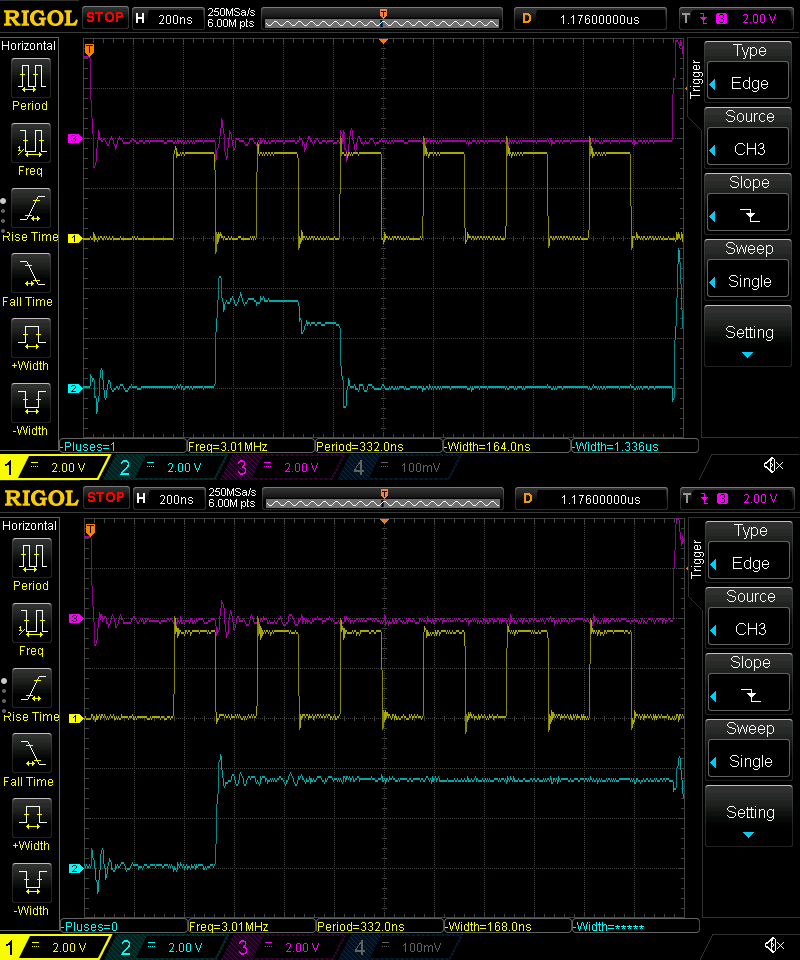
I also tried to reproduce a minimal example:
I have sent command 0xAB (Read Product ID) in qpi mode (4-4-4), then 0 or 1 dummy cycles, then read 1 byte. There are 6 dummy cycles required by flash datasheet, so flash should not write anything.
0 dummy cycles:


With resistor, 0 dummy cycles:


It seems that controller does not switch IO1 to input on the second falling edge, but instead does it on the third rising edge, where data is already being sampled.
- Mark as New
- Bookmark
- Subscribe
- Mute
- Subscribe to RSS Feed
- Permalink
- Email to a Friend
- Report Inappropriate Content
2021-09-15 8:32 AM
Nucleo-H743ZI2 with two W25Q256FV attached in dual mode (flash1 uses the very same pins as in your setup), again yellow is CLK, cyan IO2, purple NCS1. Clearly there is this intermediate level between second falling and third rising clock edge. However, this is *NOT* caused by the QSPI interface but by the flash chip itself!
The second picture shows the very same situation but only with the flash chips physically removed. No intermediate level at all, but continous high level (due to pull-ups being active).
So, yes, using SSHIFT=1 is mandatory here. The description "By default, the QUADSPI samples data 1/2 of a CLK cycle after the data is driven by the Flash memory. This bit allows the data is to be sampled later in order to account for external signal delays." is rather consistent with the present situation: The flash simply assert its data too late to be correctly sampled without this additional shift. In my setup SSHIFT=1.
BTW: To account for a yet unknown flash type, it's advisable not to use 4-4-4 mode for read id. I'd recommend to leave the flash's non-volatile configuration such that it powers up in 1-1-1 mode, then issue various "return to 1-1-1" commands (as used by different manufacturers) in 4-4-4 mode to make sure the chip reverted to 1-1-1 (in case of soft reset). Then issue RDID 0x9F in 1-1-1, and only after successful indentification switch to 4-4-4. The reason is that some devices do not support *ANY* variant of a read id command when not in 1-1-1 mode. And some others have the "nice feature" to silently revert to 1-1-1 mode when they receive 0x9F while in 4-4-4 mode ...
- Mark as New
- Bookmark
- Subscribe
- Mute
- Subscribe to RSS Feed
- Permalink
- Email to a Friend
- Report Inappropriate Content
2021-09-15 11:45 PM
Thanks for reproducing this issue, it shows that there is no problem with my specific board and/or setup.
Yet, I diagree with your conclusion about it being caused by the flash chip.
1. We both used relatively low clock speed, there is at least 180ns before falling edge and sampling. My flash requires 8ns at most, according to datasheet, I don't believe it needs an extra half cycle to assert data. Furthermore, I tried downclocking to a lowest possible speed and the issue persists. The intermediate level is rather stable and does away immediately at the rising edge.
2. I tried pulling data line directly to ground (please see comment below) and it clearly shows that stm is holding high signal after second falling edge. I bet you can try doing the same without a flash chip and verify when the line switches to input.
- Mark as New
- Bookmark
- Subscribe
- Mute
- Subscribe to RSS Feed
- Permalink
- Email to a Friend
- Report Inappropriate Content
2021-09-16 12:01 AM
Yes, you're certainly right that the QSPI interface keeps its output active longer than necessary, so that there is a conflict of QSPI and flash, both being outputs momentarily. But still I don't see any real problem there, just set SSHIFT=1, and everything works as desired.
The only problem would be using PC2_C, PC3_C and friends. They have a AMR of only 1mA, so if the output impedance of the flash is set to a sufficiently low value, this might be destructive. But on the other hand, such a conflict might easily happen anyway (even if the QSPI interface would stop driving then pin earlier) by software bug or noise, causing the QSPI interface and the flash to get "out of sync". So, these special pins should *NEVER* be used for QSPI (nor SDMMC or FMC).
- Mark as New
- Bookmark
- Subscribe
- Mute
- Subscribe to RSS Feed
- Permalink
- Email to a Friend
- Report Inappropriate Content
2021-11-21 1:00 AM
I am sorry if I interrupt this discussion. I have the very similar problem as of Ilya Balov.
This is the timing diagram of my QSPI device. And there is no dummy cycles I can add.


I did experiment with every single options of STM32F7 QUADSPI controller but it didn't work.
I suspect that the SPIO3 pin was not switched to input on time. Then the equivalent circuit of voltage divider connecting the slave output to the master output of F7 gives the weird result I guess.
I hope I can get some hint from this discussion.
Kyle