STM32F429 external nor flash data not persistent using FSMC
- Mark as New
- Bookmark
- Subscribe
- Mute
- Subscribe to RSS Feed
- Permalink
- Email to a Friend
- Report Inappropriate Content
2017-06-12 5:24 AM
Hi,
I am using STM32F429ZET6 controller in my custom board. I have used JS28F00AM29EWHA Nor flash from micron.The interface between the controller and external nor is a parallel bus. I have made FMC_Init and GPIO_Init in the following way. I have refereed the
from st for fsmc. I have also cross verified the code fromhttps://community.st.com/0D50X00009XkZtLSAV
. My issue is I get wrong manufacturer code and device_id. And also checked with the write and read functionality, but when I reset my debug session and read the previously written addresses I always get zero's. I am not getting where I am going wrong. Any help or suggestion will be of great help.https://community.st.com/community/stm32-community/stm32-forum
‌/*fsmc init as follows */
void NOR_FLASH_Init(void)
{ hnor.Instance = FMC_NORSRAM_DEVICE; hnor.Extended = FMC_NORSRAM_EXTENDED_DEVICE; hnor.Init.NSBank = FMC_NORSRAM_BANK1; hnor.Init.DataAddressMux = FMC_DATA_ADDRESS_MUX_DISABLE; hnor.Init.MemoryType = FMC_MEMORY_TYPE_NOR; hnor.Init.MemoryDataWidth = FMC_NORSRAM_MEM_BUS_WIDTH_16; hnor.Init.BurstAccessMode = FMC_BURST_ACCESS_MODE_DISABLE; hnor.Init.WaitSignalPolarity = FMC_WAIT_SIGNAL_POLARITY_LOW; hnor.Init.WrapMode = FMC_WRAP_MODE_DISABLE; hnor.Init.WaitSignalActive = FMC_WAIT_TIMING_BEFORE_WS; hnor.Init.WriteOperation = FMC_WRITE_OPERATION_ENABLE; hnor.Init.WaitSignal = FMC_WAIT_SIGNAL_DISABLE; hnor.Init.ExtendedMode = FMC_EXTENDED_MODE_ENABLE; hnor.Init.AsynchronousWait = FMC_ASYNCHRONOUS_WAIT_DISABLE; hnor.Init.WriteBurst = FMC_WRITE_BURST_DISABLE; hnor.Init.ContinuousClock = FMC_CONTINUOUS_CLOCK_SYNC_ONLY; hnor.Init.PageSize = FMC_PAGE_SIZE_NONE; /* Timing */ NOR_Timing.AddressSetupTime = 15; NOR_Timing.AddressHoldTime = 15; NOR_Timing.DataSetupTime = 10; NOR_Timing.BusTurnAroundDuration = 15; NOR_Timing.CLKDivision = 16; NOR_Timing.DataLatency = 17; NOR_Timing.AccessMode = FMC_ACCESS_MODE_B; /* ExtTiming */ ExtTiming.AddressSetupTime = 15; ExtTiming.AddressHoldTime = 15; ExtTiming.DataSetupTime = 255; ExtTiming.BusTurnAroundDuration = 15; ExtTiming.CLKDivision = 16; ExtTiming.DataLatency = 17; ExtTiming.AccessMode = FMC_ACCESS_MODE_B; /* Initialize the NOR controller */ if (HAL_NOR_Init(&hnor, &NOR_Timing, &NOR_Timing) != HAL_OK) { /* Initialization Error */ while(1); } /*♯♯-2- Read & Check the NOR device IDs ♯♯♯♯♯♯♯♯♯♯♯♯♯♯♯♯♯♯♯♯♯♯♯♯♯*/ /* Read NOR memory ID */ if(HAL_NOR_Read_ID(&hnor, &NOR_Id) != HAL_OK) { /* NOR read ID Error */ while(1); } /* Test the NOR ID correctness */ if((NOR_Id.Manufacturer_Code != (uint16_t)MANUFACTURER_CODE) || (NOR_Id.Device_Code1 != (uint16_t)DEVICE_CODE1)) { /* NOR ID not correct */ //while(1); } /*♯♯-3- Erase NOR memory ♯♯♯♯♯♯♯♯♯♯♯♯♯♯♯♯♯♯♯♯♯♯♯♯♯♯♯♯♯♯♯♯♯♯♯♯♯♯♯♯*/ /* Return to read mode */ HAL_NOR_ReturnToReadMode(&hnor);/* Erase the NOR memory block to write on */
HAL_NOR_Erase_Block(&hnor, WRITE_READ_ADDR, NOR_BANK_ADDR);/* Return the NOR memory status */
if(HAL_NOR_GetStatus(&hnor, NOR_BANK_ADDR, NOR_TIMEOUT_VALUE) !=HAL_NOR_STATUS_SUCCESS) { while(1); }}/***GPIO init **/
static void MX_GPIO_Init(void)
{ GPIO_InitTypeDef GPIO_Init_Structure; // Enable FMC clock __HAL_RCC_FMC_CLK_ENABLE();// Enable GPIOs clock
__HAL_RCC_GPIOD_CLK_ENABLE(); __HAL_RCC_GPIOE_CLK_ENABLE(); __HAL_RCC_GPIOF_CLK_ENABLE(); __HAL_RCC_GPIOG_CLK_ENABLE(); // Common GPIO configuration GPIO_Init_Structure.Mode = GPIO_MODE_AF_PP; GPIO_Init_Structure.Pull = GPIO_NOPULL; GPIO_Init_Structure.Speed = GPIO_SPEED_HIGH; GPIO_Init_Structure.Alternate = GPIO_AF12_FMC; //Data and address lines GPIO_Init_Structure.Pin = GPIO_PIN_0 | GPIO_PIN_1 | GPIO_PIN_8 | GPIO_PIN_9 | GPIO_PIN_10| GPIO_PIN_11| GPIO_PIN_12 | GPIO_PIN_13 | GPIO_PIN_14| GPIO_PIN_15; HAL_GPIO_Init(GPIOD, &GPIO_Init_Structure);GPIO_Init_Structure.Pin = GPIO_PIN_2 | GPIO_PIN_3 | GPIO_PIN_4 | GPIO_PIN_5 | GPIO_PIN_6 |
GPIO_PIN_7 | GPIO_PIN_8 | GPIO_PIN_9 | GPIO_PIN_10 | GPIO_PIN_11 | GPIO_PIN_12 | GPIO_PIN_13 | GPIO_PIN_14 | GPIO_PIN_15; GPIO_Init_Structure.Mode = GPIO_MODE_AF_PP; GPIO_Init_Structure.Pull = GPIO_NOPULL; GPIO_Init_Structure.Speed = GPIO_SPEED_HIGH; GPIO_Init_Structure.Alternate = GPIO_AF12_FMC; HAL_GPIO_Init(GPIOE, &GPIO_Init_Structure);GPIO_Init_Structure.Pin = GPIO_PIN_0 | GPIO_PIN_1 | GPIO_PIN_2 | GPIO_PIN_3 | GPIO_PIN_4 | GPIO_PIN_5 | GPIO_PIN_12 | GPIO_PIN_13 | GPIO_PIN_14 | GPIO_PIN_15;
GPIO_Init_Structure.Mode = GPIO_MODE_AF_PP; GPIO_Init_Structure.Pull = GPIO_NOPULL; GPIO_Init_Structure.Speed = GPIO_SPEED_HIGH; GPIO_Init_Structure.Alternate = GPIO_AF12_FMC; HAL_GPIO_Init(GPIOF, &GPIO_Init_Structure);GPIO_Init_Structure.Pin = GPIO_PIN_0 | GPIO_PIN_1 | GPIO_PIN_2 | GPIO_PIN_3 | GPIO_PIN_4 | GPIO_PIN_5 | GPIO_PIN_13 | GPIO_PIN_14;
GPIO_Init_Structure.Mode = GPIO_MODE_AF_PP; GPIO_Init_Structure.Pull = GPIO_NOPULL; GPIO_Init_Structure.Speed = GPIO_SPEED_HIGH; GPIO_Init_Structure.Alternate = GPIO_AF12_FMC; HAL_GPIO_Init(GPIOG, &GPIO_Init_Structure);Thanks.
#fmc #stm32f4-external-nor-flash #flash-read-and-write #js28f00am29ewha- Labels:
-
Flash
-
FMC-FSMC
-
STM32F4 Series
- Mark as New
- Bookmark
- Subscribe
- Mute
- Subscribe to RSS Feed
- Permalink
- Email to a Friend
- Report Inappropriate Content
2017-07-18 6:09 AM
>>
My issue is I get wrong manufacturer code and device_id
So what does it read? If the data bus is wrong then the chip is unlikely to recognize the commands sent to it.
Have you thoroughly reviewed the schematic design?
Up vote any posts that you find helpful, it shows what's working..
- Mark as New
- Bookmark
- Subscribe
- Mute
- Subscribe to RSS Feed
- Permalink
- Email to a Friend
- Report Inappropriate Content
2017-07-18 8:16 AM
Have you thoroughly reviewed the schematic design?
One remark for debugging: parallel memories can be easily 'bit-banged', ie. the protocol can be easily tested by 'manually' manipulating the address/data/control lines, with pins set as GPIO inputs/outputs as appropriate, rather than AF.
This can be done from the debugger, without a single line of code.
JW
- Mark as New
- Bookmark
- Subscribe
- Mute
- Subscribe to RSS Feed
- Permalink
- Email to a Friend
- Report Inappropriate Content
2017-07-19 3:25 AM
Hi Clive,
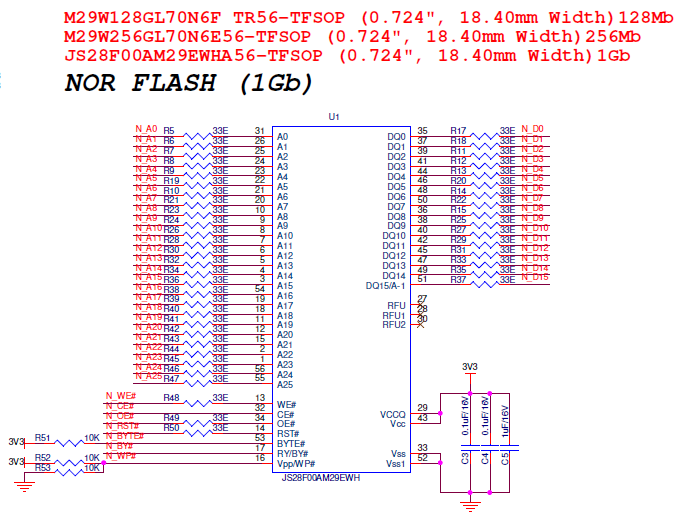
When I read the device and manufacturer id, I get both as 0x90 which is not the right value. Data and address lines are configured properly as per the schematic. Please find below schematics.

- Mark as New
- Bookmark
- Subscribe
- Mute
- Subscribe to RSS Feed
- Permalink
- Email to a Friend
- Report Inappropriate Content
2017-07-19 3:28 AM
Hi JW,
I am not getting how to proceed. Could you please elaborate on the method you mentioned in your reply.
Regards,
Shravan
- Mark as New
- Bookmark
- Subscribe
- Mute
- Subscribe to RSS Feed
- Permalink
- Email to a Friend
- Report Inappropriate Content
2017-07-19 7:33 AM
Instead of setting up the FMC and the pins for FMC, simply set all the pins connected to the memory as GPIO inputs or outputs, and manipulate them 'manually'.
This is just a way to find out whether all the connections are OK, without the risk of the FMC being misconfigured.
JW
- Mark as New
- Bookmark
- Subscribe
- Mute
- Subscribe to RSS Feed
- Permalink
- Email to a Friend
- Report Inappropriate Content
2017-07-19 7:39 AM
Hi,
Thanks for the quick response. I will check and get back to you.