- STMicroelectronics Community
- STM32 MCUs
- STM32 MCUs Products
- Re: QuadSPI instructions coming out IO1, not IO0 (...
- Subscribe to RSS Feed
- Mark Topic as New
- Mark Topic as Read
- Float this Topic for Current User
- Bookmark
- Subscribe
- Mute
- Printer Friendly Page
QuadSPI instructions coming out IO1, not IO0 (and other issues)
- Mark as New
- Bookmark
- Subscribe
- Mute
- Subscribe to RSS Feed
- Permalink
- Email to a Friend
- Report Inappropriate Content
2019-12-24 08:08 AM
So, I am getting my feet wet with QuadSPI on an STM32L412RB, talking to an external FLASH memory part (GD25Q256D, if that matters). I've got some plausible code written to "hello world" the chip, and my trusty salae hooked up, and am seeing some weird results.
I'm trying to read the "unique ID" off of the chip, which according to the chip spec requires a command of 0x4B, then four dummy bytes, then it will reply with 16 bytes of ID data. So I set up my CCR register for indirect read mode, data on 1 line, instruction on 1 line, 4 dummy cycles. No alternate bytes, no address. I assumed this makes my channel act like traditional SPI, with one line out to the part, one line in, as described in [RM0394, 15.3.4]
Single SPI mode
Legacy SPI mode allows just a single bit to be sent/received serially. In this mode, data is
sent to the Flash memory over the SO signal (whose I/O shared with IO0). Data received
from the Flash memory arrives via SI (whose I/O shared with IO1).
The different phases can each be configured separately to use this single bit mode by
setting the IMODE/ADMODE/ABMODE/DMODE fields (in QUADSPI_CCR) to 01.
In each phase which is configured in single mode:
• IO0 (SO) is in output mode
• IO1 (SI) is in input mode (high impedance)
• IO2 is in output mode and forced to ‘0’ (to deactivate the “write protect�? function)
• IO3 is in output mode and forced to ‘1’ (to deactivate the “hold�? function)
This is the case even for the dummy phase if DMODE = 01.
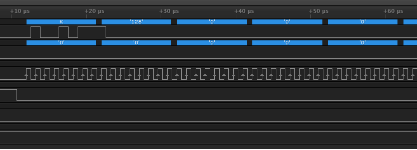
I ran the code below, and looked at the logic analyzer (figure also below). Most immediately, my instruction 0x4B seems to be coming out of IO1, aka PB1 -- not IO0, aka PB2 as I would have thought. I switched up and connected my IO1 to the IO0 (which is the input) on the flash part, same result. But this is odd. If this is a configuration issue, what would that be? If this is impossible, I will re-check my wiring for the fourth time.
Secondly, I see that my correct bytes b01001011=0x4B are being sent out, but weirdly the line stays high for an additional clock cycle, which is recognized by the analyzer as a '128' in the next byte, which is supposed to be a dummy byte. I don't know why this is, or if this is indicative of a problem, or if the parts simply don't care because its a dummy byte.
Third, my part isn't responding. The logic analyzer looks just like the FLASH part spec, but I have not ever received anything from the MISO yet, flatlined. This is before and after trying to switch up my MISO and MOSI, per my IO1 confusion above.
Anyway, if anybody notices any rookie mistakes below, please let me know. As always, very much appreciate the help.
Initialization code:
void qspi_init(void)
{
    uint32_t tmpreg;

    //////////////////////////////////////////////////
    // Configure GPIO for QUADSPI
    // PB10 = QUADSPI_CLK (alternate function 10)
    // PB11 = QUADSPI_BK1_NCS (alternate function 10)
    // PB2  = QUADSPI_BK1_IO0 (alternate function 10)
    // PB1  = QUADSPI_BK1_IO1 (alternate function 10)  commands coming out here
    // PA7  = QUADSPI_BK1_IO2 (alternate function 10)
    // PA6  = QUADSPI_BK1_IO3 (alternate function 10)
    // [RMM0394, 8.4], [DS12469, Table 16]
    // (Note: QUADSPI_CLK can alternatively be put on PA3,
    // and QUADSPI_BK1_NCS can be put on PA2)
    //////////////////////////////////////////////////

    const uint8_t Q_GPIO_MODE        = 0x2;  // the mode is b10, alternate function [RMO394 8.4.1]
    const uint8_t Q_GPIO_OTYPE       = 0x0;  // output push-pull
    const uint8_t Q_GPIO_OSPEED      = 0x3;  // very high speed
    const uint8_t Q_GPIO_PUPD_CS     = 0x1;  // pull up for CS
    const uint8_t Q_GPIO_PUPD_OTHERS = 0x0;  // no pull-up for others
    const uint8_t Q_GPIO_AFR         = 0xA;  // alternate function 10

    GPIO_Init(GPIOB, GPIO_PIN_11,                           Q_GPIO_MODE, Q_GPIO_OTYPE, Q_GPIO_OSPEED, Q_GPIO_PUPD_CS, Q_GPIO_AFR);
    GPIO_Init(GPIOA, GPIO_PIN_6 + GPIO_PIN_7,               Q_GPIO_MODE, Q_GPIO_OTYPE, Q_GPIO_OSPEED, Q_GPIO_PUPD_OTHERS, Q_GPIO_AFR);
    GPIO_Init(GPIOB, GPIO_PIN_1 + GPIO_PIN_2 + GPIO_PIN_10, Q_GPIO_MODE, Q_GPIO_OTYPE, Q_GPIO_OSPEED, Q_GPIO_PUPD_OTHERS, Q_GPIO_AFR);

    //////////////////////////////////////////////////
    // Enable the IO port A and B clocks [RMM0394, 6.4.16]
    //////////////////////////////////////////////////

    RCC->AHB2ENR |= (1 << 0);  // set AHB2ENR[0], IO port A clock enabled
    tmpreg = (RCC->AHB2ENR & (1 << 0)); // read it back to delay

    RCC->AHB2ENR |= (1 << 1);  // set AHB2ENR[1], IO port B clock enabled
    tmpreg = (RCC->AHB2ENR & (1 << 1)); // read it back to delay

    /////////////////////////////////
    // enable the quadspi peripheral clock [RM0394 rev4, 6.4.17]
    /////////////////////////////////

    RCC->AHB3ENR |= (1 << 8);  // set AHB3ENR[8], quadspi clock enabled
    tmpreg = (RCC->AHB3ENR & (1 << 8)); // read it back to delay

    /////////////////////////////////
    // force and release the QSPI memory interface [RM0394 rev4, 6.4.11]
    /////////////////////////////////

    RCC->AHB3RSTR |= (1 << 8);
    RCC->AHB3RSTR &= ~(1 << 8);

    #define AHB_PRESCALER_MINUS_ONE (100)

    QUADSPI->CR =
        AHB_PRESCALER_MINUS_ONE << QUADSPI_CR_PRESCALER_Pos // F_CLK = F_AHB/3 (72MHz when CPU is 216MHz)
        | 3 << QUADSPI_CR_FTHRES_Pos // 4 bytes must be available to read/write
        #if defined(QUADSPI_CR_FSEL_Pos)
        | 0 << QUADSPI_CR_FSEL_Pos // FLASH 1 selected
        #endif
        #if defined(QUADSPI_CR_DFM_Pos)
        | 0 << QUADSPI_CR_DFM_Pos // dual-flash mode disabled
        #endif
        | 0 << QUADSPI_CR_SSHIFT_Pos // no sample shift
        | 1 << QUADSPI_CR_TCEN_Pos // timeout counter enabled
        | 1 << QUADSPI_CR_EN_Pos // enable the peripheral
        ;

    QUADSPI->DCR =
        (24 - 3 - 1) << QUADSPI_DCR_FSIZE_Pos
        | 1 << QUADSPI_DCR_CSHT_Pos // nCS stays high for 2 cycles
        | 0 << QUADSPI_DCR_CKMODE_Pos // CLK idles at low state
        ;
}
Code to read the unique ID from the external FLASH part. This is supposed to be comprised of an instruction of 0x4B, then four dummy cycles, and then 16 bytes of ID data returned from the part. (As it happens, nothing is returned.)
void qspi_test_ReadUniqueID(void)
{
    // assume 3 byte mode
    // which means 4 dummy bytes

    QUADSPI->DLR = 16 - 1; // number of bytes to read

    QUADSPI->ABR = 0; // alternate byte: disable continuous read mode

    QUADSPI->CCR =
        0 << QUADSPI_CCR_DDRM_Pos // DDR mode disabled
        | 0 << QUADSPI_CCR_SIOO_Pos // send instruction every transaction
        | 1 << QUADSPI_CCR_FMODE_Pos // indirect read mode
        | 1 << QUADSPI_CCR_DMODE_Pos // data on 1 line
        | 4 << QUADSPI_CCR_DCYC_Pos // 4 dummy cycles
        | 0 << QUADSPI_CCR_ABMODE_Pos // no alternate byte
        | 0 << QUADSPI_CCR_ADMODE_Pos // no address
        | 1 << QUADSPI_CCR_IMODE_Pos // instruction on 1 line
        | 0x4B << QUADSPI_CCR_INSTRUCTION_Pos // quad read opcode
        ;
}- Labels:
-
Documentation
-
QSPI
-
STM32L4 Series
- Mark as New
- Bookmark
- Subscribe
- Mute
- Subscribe to RSS Feed
- Permalink
- Email to a Friend
- Report Inappropriate Content
2019-12-24 08:41 AM
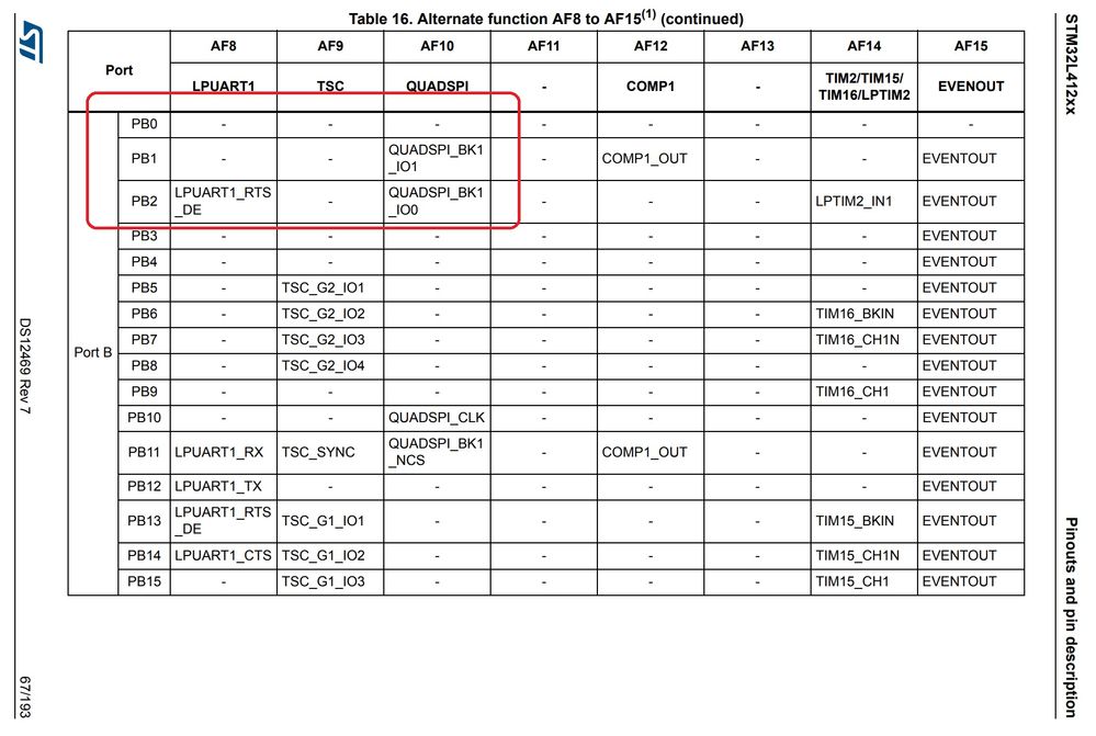
PB2 is uninvolved, PB1 is BK1_IO0, and PB0 is BK1_IO1, see the pin lists, not the AF table
The table of page 67 is wrong
https://www.st.com/resource/en/datasheet/stm32l412rb.pdf
Up vote any posts that you find helpful, it shows what's working..
- Mark as New
- Bookmark
- Subscribe
- Mute
- Subscribe to RSS Feed
- Permalink
- Email to a Friend
- Report Inappropriate Content
2019-12-24 08:45 AM
@Amel NASRI @Imen DAHMEN This QUADSPI column is off-by-one
COMP1_OUT should be on PB0
LPUART1_RTS_NE and LPTIM2_IN should be on PB1
LPTIM1_OUT on PB2
PB4 is wrong, PB5 is wrong
PB10/PB11 for QUADSPI looks correct
Whole table on this page needs a thorough review and validation
Up vote any posts that you find helpful, it shows what's working..
- Mark as New
- Bookmark
- Subscribe
- Mute
- Subscribe to RSS Feed
- Permalink
- Email to a Friend
- Report Inappropriate Content
2019-12-25 11:04 AM
Oh my gosh clive, thanks so much. That worked. How did you discover this mistake, just superhuman attention to detail?
Merry christmas!
- Mark as New
- Bookmark
- Subscribe
- Mute
- Subscribe to RSS Feed
- Permalink
- Email to a Friend
- Report Inappropriate Content
2019-12-25 11:54 AM
Merry Christmas
The pin assignment looked odd, based on other STM32, so I cross checked the list vs table.
Up vote any posts that you find helpful, it shows what's working..
- Mark as New
- Bookmark
- Subscribe
- Mute
- Subscribe to RSS Feed
- Permalink
- Email to a Friend
- Report Inappropriate Content
2019-12-27 06:30 AM
Hello,
Your reported issue is raised internally for review and correction.
I wish you a merry Christmas and Happy New year !
Best Regards,
Imen
Thanks
Imen
- Mark as New
- Bookmark
- Subscribe
- Mute
- Subscribe to RSS Feed
- Permalink
- Email to a Friend
- Report Inappropriate Content
2019-12-27 06:55 AM
Thanks
Up vote any posts that you find helpful, it shows what's working..
- How to UNinstall stm32cubeide, stm32cubeProgrammer, stm32trusted package installer in STM32CubeIDE (MCUs)
- QSPI RAM on OSPI Interface of H7A3 MCU issues in STM32 MCUs Products
- STM32N6: MPU config, code execution - why not at 0x70000000? in STM32 MCUs Products
- Block Erase Function Issue with MT25QL01GBBB NOR Flash on STM32 MCU in STM32 MCUs Products
- STM32U5A5 Jump to Bootloader from ThreadX Application with TrustZone enabled in STM32 MCUs Embedded software

