Get ready for the STM32 Summit 2026 | Online, November 3
Join discussions in the Product Forums. Ask questions, learn from your peers, and share insights on ST solutions to accelerate your design journey.
Most recent activity
Hi ST,Today I decided to give STM32CubeIDE for VS Code another try.I installed all 15 latest packages (Rev. 3.10).Using the STM32Cube Bundle Manager, I installed all required bundles, including Ninja 1.13.2.After opening in VS Code the folder containing the code generated by STM32CubeMX (CMake option) and trying to configure CMake for the first time (Ctrl+Shift+P → CMake: Configure), I received the error below.What am I missing? The last time I tried this several months ago, the project at least configured correctly and built successfully. Kind regards,Thomas [main] Configuring project: Firmware[driver] NOTE: You are configuring with preset Debug, but there are some overrides being applied from your VS Code settings.[proc] Executing command: "C:\Program Files (x86)\Microsoft Visual Studio\2022\BuildTools\Common7\IDE\CommonExtensions\Microsoft\CMake\CMake\bin\cmake.exe" -DCMAKE_BUILD_TYPE=Debug -DCMAKE_TOOLCHAIN_FILE=C:/Projects/All-purpose-Micro-Controller-2/Firmware/cmake/gcc-arm-none
STM32CubeIDEI have Project Directory (Fully populated from an earlier version of the IDE on a different machine)that I bundled up and then unwrapped on my new build machine.However, when I point my newly installed (up to date) IDE to my unwrapped Project directory,it “sees” the Project is there...but when I click “Finish” to bring it into my IDE, the IDE showsthe project (with the correct name) but devoid of any project properties...and no Source Code Tree(where I normally--and previously--could navigate all the source files). I can see all the expected source code files in my Project DirectoryWhat is the disconnect?Do I need to manually edit the PROJECT.ioc or .project file (or .cproject or .settings or *something*) ?Is there a known issue with transferring a Project from an earlier version of the IDE?Guidance Appreciated!Paul++
Hello,We have designed a custom RF module based on the STM32WL33, and one of ourcustomers is asking us to demonstrate that the RX sensitivity of our modulematches the values published in the datasheet: - RX sensitivity @ 1% BER: -132 dBm @ 300 bit/s, 433 MHz, OOK -128 dBm @ 300 bit/s, 868 MHz, 2(G)FSK -112 dBm @ 38.4 kbit/s, 868 MHz, 2(G)FSKTo validate this, we would like to reproduce the exact test conditions usingan official ST development board (e.g. NUCLEO-WL33) and theSTM32WL33 GUI, so the result is directly comparable to thedatasheet.In the GUI's "Radio settings" tab we can set: fc, DR (ksps), Fdev (kHz),CHF (channel filter bandwidth, kHz), modulation (OOK/2(G)FSK/4(G)FSK/ASK),Spread Factor, and Pout.Could you please help us with the following:1. What DR / Fdev / CHF / Spread Factor values did ST use internally to characterize each of the three sensitivity points above? In particular: - For -132 dBm @ 300 bit/s / 433 MHz / OOK: Under the test conditions of 1
Hello! I installed the extension and configured it to work through a proxy (downloading the compiler, etc.), and everything works fine, but when I try to download devices list via cube pack sync, I get the error: Failed to download with Unsupported `GLOBAL_AGENT.HTTP_PROXY` configuration value: URL protocol must be "http:" I tried adding the proxy via platform environment variables, but that didn't help. Platform: Win11 IDE pluggin: 3.6.4 Pack manager: 0.3.12
Dear Community,I am currently following the official MEMS Studio tutorial "Module 5 - MLC Configuration and Visualization" available on YouTube.I am using the following hardware and software setup:MEMS Studio version: 2.4.0 Board: NUCLEO-F401RE with X-NUCLEO-IKS4A1I was able to successfully complete all tutorial steps up to the Automatic Filter & Feature Selection (AFS) stage. However, whenever I click "Run" in the AFS tool, MEMS Studio displays the following error message:"Unexpected error with code 104 occurred during AFS request processing."The issue occurs consistently, even though I am following the tutorial exactly as shown in the video.Additional information:The PC has internet access. I tested both my company network and a mobile hotspot, but the error persists in both cases. No firewall events indicating blocked connections were detected. The board is correctly recognized by MEMS Studio and all previous steps work as expected.Could you please help me identify the cause of
Hello ST Community,I would like to report a bug in the code generated by STM32CubeMX 6.17.0 for the STM32WBA55 with firmware package STM32Cube FW_WBA V1.9.0. Environment- MCU: STM32WBA55CGU6- CubeMX: 6.17.0- Firmware package: STM32Cube FW_WBA V1.9.0- Toolchain: Keil MDK-ARM V5.37- Middleware: STM32_WPAN (BLE Basic stack) Problem descriptionThe application crashes with a HardFault after approximately 2 minutes of operation. The fault is caused by a NULL function pointer call in the generated file `Utilities/tim_serv/STM32_timer.c`, inside `UTIL_TIMER_IRQ_Handler`. Suggested fixAdd a NULL guard before the callback invocation in `UTIL_TIMER_IRQ_Handler`:if( currentExecutionHead->Callback != NULL ) { currentExecutionHead->Callback(currentExecutionHead->argument);} NoteThis issue appeared after migrating from FW_WBA V1.6.1 to FW_WBA V1.9.0. The same project worked correctly with the previous version.
I'm configuring SAI4 (Block A) to receive I2S audio from an external microphone (Knowles SPH0645), using HPDMA3 for continuous circular DMA transfer, targeting the Cortex-M33 (Cube) context.Configuration so far:SAI4 → SAI A → Mode: Master, I2S/PCM Protocol, Audio Mode: Master Receive, Data Size: 24 bits, Mono HPDMA3 Channel (currently CH2) → Request: SAI4_A Circular Mode: Enable Direction: Peripheral To Memory Priority: HighProblem:The field "DMA Handle in IP Structure" under Request Configuration shows a red ⊗ error icon, with the value stuck as a placeholder. When I try to click the dropdown to select a proper handle (e.g. DMA_Handle1, DMA_Handle2), the available options appear grayed out / not selectable — I cannot click or choose any of them. This leaves the field marked invalid (red cross), which propagates up to the HPDMA3 channel, CH tab, and Features tab all showing red crosses.I confirmed:SAI4's runtime context is properly checked (currently testing M33NS) The Request field co
Hi,I am working on a Matter-over-Thread firmware project on the NUCLEO-WBA65RI / STM32WBA65RIVx, and I am seeing an issue where the Amazon Alexa app does not detect the board during Matter commissioning.My current environment is: Board: NUCLEO-WBA65RI MCU: STM32WBA65 STM32Cube FW_WBA: V1.9.0 X-CUBE-MATTER: V1.6.0 STM32CubeIDE: 1.17.x Commissioner being tested: Amazon Echo 4th Gen, model L4S3RE Matter / connectedhomeip version: v1.3.0 as packaged in X-CUBE-MATTER V1.6.0 The device boots correctly, Thread and Matter initialize, and the commissioning window opens. From UART logs I can confirm: Thread task starts successfully Matter task starts successfully BLE stack initializes successfully Matter BLE advertising starts Matter service UUID 0xFFF6 is present in the advertising payload Manual pairing code and QR payload are generated Fabric count is 0 Commissioning window opens successfully The device is also visible in BLE scanner tools such as nRF Connect. nRF Co
Hello,I am trying to create an FSBL XIP project for the NUCLEO-N657X0-Q with the following structure: FSBL running from internal SRAM Application executing in place from the external XSPI flash ThreadX and NetX Duo running in the Application context Ethernet using the onboard LAN8742 PHY External Memory Loader project The STM32CubeN6 firmware package contains two relevant examples: Projects/NUCLEO-N657X0-Q/Templates/Template_FSBL_XIP Projects/NUCLEO-N657X0-Q/Applications/NetXDuo/Nx_UDP_Echo_Client However, the two examples use different project structures.Template_FSBL_XIP provides the required FSBL, XIP Application, and External Memory Loader structure, but it does not contain the ThreadX, NetX Duo, and Ethernet application configuration.Nx_UDP_Echo_Client, on the other hand, contains the required ThreadX, NetX Duo, Ethernet, LAN8742, and UDP configuration, but the complete application is assigned to the FSBL context instead of being built as a separate XIP Application.Copyi
Hi,I struggled a while to find out why my STM8S I2C was always “Busy”.Even AI had some headaches (except only one put me on the track ...)This device requires to configure the definition of I2C pinout in special FLASH.To do this, compile your project and open ST Visual Programmer.Load your “My_project.s19” file. There are three TABS in the window: PROGRAM MEMORY, DATA MEMRORY and OPTION BYTE. Click on option byte, select AFR6 and change it for “I2C SDA SCK” instead of “AIN4 AIN5”. Save your “My_project.s19” file.When your will burn the device, it will write the new parameters in the FLASH and the device will always be configured for I2C. You do this exercise only once.Hope it will help ….
Hi, I'm seeing a consistent issue where every sensor connected via I²C (as far as I can tell) produces 0 bytes of streamed data over USB:HTS221 (temperature + humidity) LPS22HH (pressure + temperature) STTS751 (temperature) IIS2MDC (magnetometer)At the same time, all SPI-based sensors stream normally:IIS3DWB IIS2DH ISM330DHCX (accelerometer + gyroscope)Both microphones also work correctly.Execution details:Board: STEVAL-STWINKT1BFirmware package: FP-SNS-DATALOG1 v1.5.1 (Utilities/HSDPython_SDK included)Host SDK: HSDPython_SDK (st_hsdatalog 3.0.1, st_dtdl_gui 2.1.0, st_pnpl 2.1.0), Python 3.10, Windows 10Connection: USB (WinUSB), using hsdatalog_cli.pyResult (consistent across multiple runs and after a full USB power-cycle of the board):Name Length---- ------AcquisitionInfo.json 226DeviceConfig.json 28090HTS221_HUM.dat 0HTS221_TEMP.dat 0IIS2DH_ACC.dat 76608IIS2MDC_MAG.dat 0IIS3DWB_ACC.dat 1542000IM
The test conditions of VINCL parameters of VNS3V04DPTR-E chip are: Does light inject 1mA current into the IN pin, and does the SOURCE pin need to be grounded?
Hi community,I am using yocto build ( version - openstlinux-6.6-yocto-scarthgap-mpu-v25.06.11) in this I am facing challenge over below build time error.Exception: subprocess.CalledProcessError: Command 'tar --exclude=./sysroot-only -cf - -C .../linux-libc-headers/6.6/image -p -S . | tar -xf - -C .../linux-libc-headers/6.6/package' returned non-zero exit status 2. got *at() syscall for unknown directory, fd 4 unknown base path for fd 4, path include couldn't allocate absolute path for 'include'. function package_prepare_pkgdata finished DEBUG: Executing python function perform_packagecopy ERROR: Error executing a python function in exec_func_python() autogenerated:The stack trace of python calls that resulted in this exception/failure was: File: 'exec_func_python() autogenerated', lineno: 2, function: <module> 0001: *** 0002:perform_packagecopy(d) 0003: File: '/home/datadir/EVK-build-CMS/layers/openembedded-core/meta/classes-global/package.bbclass', lineno: 363, function: perform
The magnetometer doesn’t start over I2C and doesn’t output data via UART. Please help solve the problem; the files are attached.
I recently purchased the STEVAL-LLL001V1 evaluation board, which uses the STLED524 LED driver. According to the user manual (UM2143), the board requires the software STLED524_V1.44.exe (or a later version) for operation. However, I have been unable to locate this software.Could you please let me know where I can download it?
Hi everybody,I’m struggling with the lwip stack in order to get it working with freertos.I had succesfully achieved to bring up the connection and optain an ip in dhcp mode and ping the board in bare metal mode, now I switched to freertos and I’m no longer able to send discovery packets on the network.I followed the instructions stated here stm32-hotspot/STM32H7-LwIP-Examples: Ethernet examples using LwIP + FreeRTOS for STM32H7 Discovery and Nucleo boards and tried to copy .ioc configuration from H745 example but I still have the same problem, the phy connection goes up but I cannot obtain the IP address from dhcp server. I’m monitoring the network activity with wireshark but there is nothing coming from the board mac address (in bare metal mode I was able to see dhcp negotiations).Please find the attached files in order to check what happens and addres the possible issue.My configuration: STM32CubeIDE Version: 2.2.0STM32CubeMX Version: 6.17.0STM32Cube FW_H7 V1.13.0PS: please note that
Hi ,I generated a new STM32F407 project using STM32CubeMX.However, I cannot find I-CUBE-LRWAN under Software Packs or Middleware for the STM32F407G-DISC1 board.From what I understand, CubeMX only exposes I-CUBE-LRWAN for certain STM32 devices such as:STM32WL series B-L072Z-LRWAN1 Discovery Kit Some STM32L0/L4 examplesbut not for STM32F407.Because of this, I am unsure about the correct integration method.What I have DoneCreated a new STM32F407G-DISC1 project in STM32CubeMX. Configured the required peripherals (SPI, UART, GPIO, RTC, etc.). Added the SX1262 driver from the following repository: https://github.com/Saba-abiri/LORA1262 Identified and copied the required I-CUBE-LRWAN source files into my STM32F407 project. Resolved most of the compilation errors after integrating the middleware. Successfully built the project.Although the project now builds successfully, I am still unsure whether the middleware has been ported correctly because the LoRaWAN stack does not appear to initializ
I have a custom design with STM32mp135f + MT41K256M16TW-107 DDR3L @ 533MHz that I want to bring up. I built a Linux image based on OpenSTLinux guides and it boots until my kernel is loaded (uboot logs : “starting kernel”) then its crashes without any logs even with earlycon. By testing the DDR with ST DDR Tool, I realized that byte-masked writes fail (test 9), but halfword & RMW32 work. I noticed the byte lane swap but it is identical on the dk board. I am a bit lost and don’t know if the issue is timing/config related or due to my hardware design.
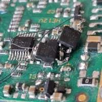
Good morning,I'm working on some new automotive designs and on the current boards i found what are , presumibly, STM components but i can't really identify them with the offerings in the online catalogs, (at least IF they are STM engineering samples)The body is specifically PowerSSO-16 but the marking of the components i found for now present similar but very different top markings2HTS90 D1B1HTS20 D11HTS10 200U2HTS30 D1B1HTS50 D1(these 5 are the ones i classified so far) Can i have some help in documenting them, if they indeed are VND productsBellow a picture of one of the components, there are all the same except the top markings (no logos or such)
Dear Team,I am facing an issue while programming an STM32H533 device using the ST-LINK V3SET. I have observed different behavior depending on the compiler optimization level and programming interface. The details are provided below.Case 1 – Flash Programming FailurePlease find the debug log below:-------------------------------------------------------------------STM32CubeProgrammer v2.20.0-------------------------------------------------------------------Log output file: C:\Users\29397\AppData\Local\Temp\STM32CubeProgrammer_a36804.logST-LINK SN : 0042001A3234510537333934ST-LINK FW : V3J17M11B6S1Board : STLINK-V3SETVoltage : 0.00VSWD freq : 8000 KHzConnect mode: Under ResetReset mode : Hardware resetDevice ID : 0x478Revision ID : --Device name : STM32H533/523Flash size : 512 KBytesDevice type : MCUDevice CPU : Cortex-M33BL Version : 0xE2SFSP Version: v1.2.0Debug in Low Power mode enabledOpening and parsing file: ST-LINK_GDB_server_a36804.srecMemory Programming ...File : ST-LINK_GDB_serv
What is the correct way to implement multiple ADC channels? I have tried various tutorials on YouTube, but none of them work correctly. I am using two potentiometers. The ADC readings are random and cannot be controlled by the potentiometers. At one point, I managed to get it working, but only one potentiometer responded. The second potentiometer did not work, and the value of Channel 2 followed the value of Channel 1, even though Channel 2 should be controlled independently by the second potentiometer.
Hello,We are designing a custom board using the STM32MP157FAC1 device. For programming and debugging, we are providing an STDC14 connector on our board and use the STLINK-V3SET debugger/programmer.As per AN5031 (Section 8.3.3), the recommended ESD protection device is ESDALC6V1W5. Snapshot is attached for kind reference.We have the following queries:Query 1:Can we use the HSP053-4M5 device instead of the ESDALC6V1W5 for ESD protection? We are already using the HSP053-4M5 to protect the data, clock, and command lines of the microSD card interface. Using the same device for the STDC14 interface would help us optimize the BOM.Query 2:Can we connect USART1_TX (PA9) and USART1_RX (PB15) of the STM32MP157FAC1 to Pin 14 (T_VCP_TX) and Pin 13 (T_VCP_RX), respectively, on the STDC14 connector for the STLINK-V3SET Virtual COM Port interface? Regards,PS
Hi, I’m using Nucleo-64 development board with STM32H533RE. On the board,H533:RTC crystal is Crystal, 32.768kHz, 9pF, +/-20ppm, 70KR, 1.6x1mm and load capacitors are 3.9pF each.Crystal 24MHz, 6pF, +-20ppm, 80ohms max, SMD, and load capacitors are 6.8pF each. F723:on the same board, the STM32F723IEK6, it is Crystal, 24MHz, 6pF, +/-20ppm, 80R, 2x1.6mm and load capacitors are 2.7pF each.should the RTC load capacitor value close to 15pF each? should be 24Mhz load capacitors close to 10pF each? why STM32F7 and STM32H5 24MHz have different capacitor values?Thank you for your concerns
I’m designing another PCB for the STM32L452 LQFP48, and I was wondering - how big is the die? Can I see a picture of the structure of the LQFP 48 before it is encapsulated?I use double layer boards, and have as much ground plane under the micro, both top and bottom layer as possible. But I often sneak some power tracks around the inside perimeter of the micro. But under the plastic goo I do not know how big the die is. How far can I go with tracks before I am under the actual microprocessor? I think knowing the internal dimensions of the package would help me fine tune my printed circuit board designs.I suppose I could destroy one to find out, but that seems like a waste (and messy). I can’t imagine it would be company confidential… or could it? If a photo is confidential, how about a CAD drawing? … or maybe an artist’s impression...
Heyho,just played with / checked the FPU on a G431.I found that the CubeIDE setting overrides the enable via register SCB->CPACR.So, if source code sets FPU on, but IDE says FPU off, the FPU is off.That a bug or a feature?
Already have an account? Login
Enter your E-mail address. We'll send you an e-mail with instructions to reset your password.