Associate
July 24, 2026
Question

STM32MP135 DDR3 DQM Write Mask Failure (Byte writes only)

  • July 24, 2026
  • 6 replies
  • 73 views

I have a custom design with STM32mp135f + MT41K256M16TW-107 DDR3L @ 533MHz that I want to bring up. I built a Linux image based on OpenSTLinux guides and it boots until my kernel is loaded (uboot logs : “starting kernel”) then its crashes without any logs even with earlycon. By testing the DDR with ST DDR Tool, I realized that byte-masked writes fail (test 9), but halfword & RMW32 work. 
 

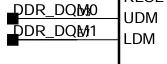
I noticed the byte lane swap but it is identical on the dk board. I am a bit lost and don’t know if the issue is timing/config related or due to my hardware design. 
 

6 replies

mƎALLEm
ST Technical Moderator
July 24, 2026

Hello ​@TP1 and welcome to the ST community,

You have posted your thread in a wrong forum board (STM32 MCUs Boards and hardware tools). Your question is about a MPU product.

I moved your post to “STM32 MPUs Products and hardware related” forum board.

Good luck.


To give better visibility on the answered topics, please click "Best answer" on the reply which solved your issue or answered your question.
PatrickF
ST Employee
July 27, 2026

Hi ​@TP1 ,

could you share the complete MP13/DDR3L schematic parts where we could see all DDR signals as with only the information above there is still possibility of wrong swap (data/DQS/DQM should always be together). 

Regards.


In order to give better visibility on the answered topics, please click on 'Best Answer' on the reply which solved your issue or answered your question.Tip of the day: Try Sidekick STM32 AI agent
TP1Author
Associate
July 27, 2026

Hi ​@PatrickF,


Here is the DDR schematic :

From what I can tell, it looks similar to the layout of stm32mp135f-dk but the DDR models are different. 


Thank you for your help,


Regards.

PatrickF
ST Employee
July 27, 2026

Hi ​@TP1 

unfortunately, what I see in your schematics is wrong and explain you byte write issues.

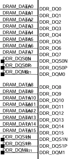
You did not wired the same bytes mask/strobe with associated byte data:

  • MP13 DQM0/DQS0 (DQ0-DQ7 Lower bytes write Data Mask/Data Strobe) to DDR3L UDM/UDQS (DQ15-8 Upper byte write Data Mask/Sata Strobe). This requires the data byte to be also swapped.
  • but you wired MP13 DATA0-DATA7 (Lower byte) to DDR3L DQ0-DQ7 (Lower byte)


No way to solve that by SW setting, you should correct your PCB.

see example on MP135F-DK board
MP13 side:

DDR3L side: 


Regards.

In order to give better visibility on the answered topics, please click on 'Best Answer' on the reply which solved your issue or answered your question.Tip of the day: Try Sidekick STM32 AI agent
TP1Author
Associate
July 27, 2026

Thank you ​@PatrickF for your help.
Would this rewiring be correct if I don’t swap the DQ0-DQ7 and DQ8-DQ15 data lanes ?
 

DQM0 <-> LDM
DQM1 <-> UDM
DDR_DQS0P <-> LDQS

DDR_DQS0N <-> LDQS#

DDR_DQS1P <-> UDQS

DDR_DQS1N <-> UDQS#


Regards.

PatrickF
ST Employee
July 27, 2026

Yes, this would be ok.

You should take DQ0/DQS0/DQM0 (or their alternate names LDQ/LUDM) as a 10 signals group which must be altogether. and similarly for other byte. 
DDR3L don’t care about lower or higher byte meanings, but all bytes related signals should be on same byte.

Regards.


In order to give better visibility on the answered topics, please click on 'Best Answer' on the reply which solved your issue or answered your question.Tip of the day: Try Sidekick STM32 AI agent