- STMicroelectronics Community
- STM32 MCUs
- STM32 MCUs Products
- STM32H755, is the clock too slow?
- Subscribe to RSS Feed
- Mark Topic as New
- Mark Topic as Read
- Float this Topic for Current User
- Bookmark
- Subscribe
- Mute
- Printer Friendly Page
STM32H755, is the clock too slow?
- Mark as New
- Bookmark
- Subscribe
- Mute
- Subscribe to RSS Feed
- Permalink
- Email to a Friend
- Report Inappropriate Content
2024-02-13 2:10 AM
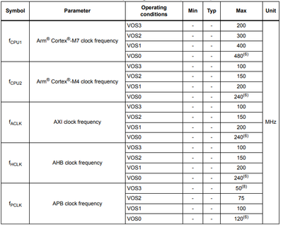
Hello everyone, I'm working on an STM32H755BI (industrial temperature range), and i'm quite disappointed by the maximum clock reachable from the system.
As can be seen, the MCU can reach up to 480MHz in the core M7 and 240MHz in the core M4.
After months of develpment, a firmware package update blocked me the VOS0 and VOS1, and in fact reading the user manual those modes are unavailable on my package, so i reduced to 300MHz and 150MHz
Today, with an update of cube MX, this error appeared in the clock tree:
And in fact by reading the datasheet APB4 is limited to 100MHz.
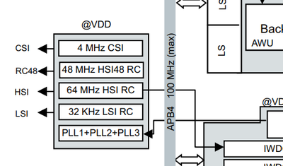
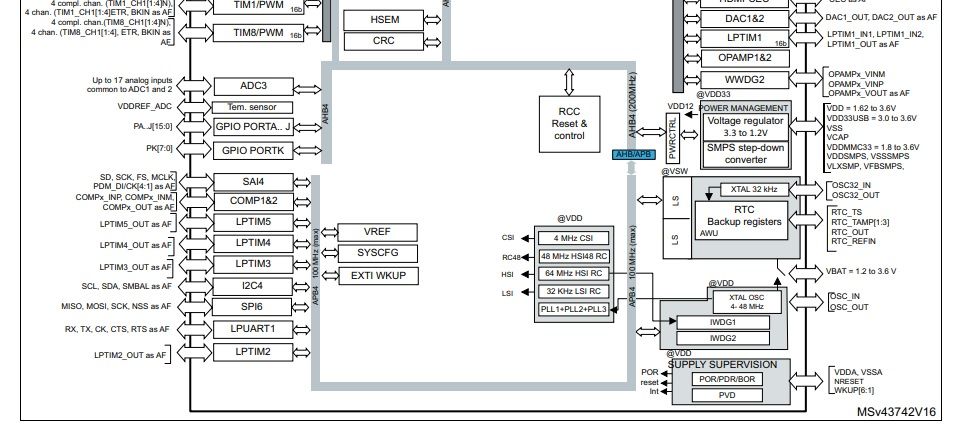
Reducing APB4 to 100MHZ could not be a big deal, but the real problem is that considering the clock distribution in the previous image the clock of the APB4 is the same clock of the M4 (CPU2).
Does this means that i bought a 480+240MHz and i'm forced to use it at 300+100 after more than a year of development?
- Labels:
-
Power
-
RCC
-
STM32CubeMX
-
STM32H7 series
- Mark as New
- Bookmark
- Subscribe
- Mute
- Subscribe to RSS Feed
- Permalink
- Email to a Friend
- Report Inappropriate Content
2024-02-13 4:30 AM
Dear @halbeeee ,
We have a specific application Note that explains the STM32H7 MCU Life time STM32H7 Series lifetime estimates - Application note : AN5337, depending on the Operation ratio of RUN/Low power modes and also Temperature .
Let me know how I can help you on your particular case to optimize it further.
Cheers,
STOne-32
- Mark as New
- Bookmark
- Subscribe
- Mute
- Subscribe to RSS Feed
- Permalink
- Email to a Friend
- Report Inappropriate Content
2024-02-13 4:54 AM
Sorry, but i didn't get the point of your comment. How can my problem and the application note you posted be related?
- Mark as New
- Bookmark
- Subscribe
- Mute
- Subscribe to RSS Feed
- Permalink
- Email to a Friend
- Report Inappropriate Content
2024-02-13 5:52 AM - edited 2024-02-13 5:52 AM
Interesting.
The reference manual says it can do 480 MHz. It would be odd for the datasheet to have such a large error. The H745/H755 has been out for a while and is clearly advertised as 480 MHz capable. I would be surprised if it were only capable of 300 MHz.
The CubeMX folks tend to follow the datasheet, so it's not surprising that CubeMX flags the error.
The restriction seems to only be listed in that one figure. In many other places in the manual, it says CPU2 can run at 240 MHz, so that's not very consistent.
On the other hand, there is this note in the datasheet which suggests the change was intentional:
Nothing relevant in errata sheet.
Perhaps @STOne-32 can look a little more closely at this.
- Mark as New
- Bookmark
- Subscribe
- Mute
- Subscribe to RSS Feed
- Permalink
- Email to a Friend
- Report Inappropriate Content
2024-02-13 5:58 AM
It has a direct link on the maximum Frequency of the CPU and on the VOSx depending on the temperature. In order to understand correctly your application use case, do you know what is the expected operating temperature ? For instance to reach 450MHz for M7 , VOS0 is a must , however limited to junction temperature up to 105 degrees Celsius.
- Mark as New
- Bookmark
- Subscribe
- Mute
- Subscribe to RSS Feed
- Permalink
- Email to a Friend
- Report Inappropriate Content
2024-02-13 6:07 AM
@TDK Thank you for the reply. The maximum clock was reduced to 300MHz with the FW package 1.11.0 if i'm not wrong. But the datasheet confirms this maximum value of 300MHz and there is nothing to do. The reliability is a crucial requirements so i have to follow the requirements.
I also think that your pointed note refers to VOS3 (or at least i hope, since FCPU2 of 150MHz is allowed by cube)
@STOne-32 My problem is not the reduction from 480 to 300 MHz due to the VOSx settings, but the new limit in the APHB that blocks the CPU2 from reaching frequencies allowed by the current VOSx settings, limiting it from a theoretical 240Hz to a maximum of 100MHz.
- Mark as New
- Bookmark
- Subscribe
- Mute
- Subscribe to RSS Feed
- Permalink
- Email to a Friend
- Report Inappropriate Content
2024-02-13 6:17 AM
Not sure the plumbing is consistent with how it used to be.
APB4 used to be fractional from the AHB clock (M4 CPU), so M7 400 MHz, AHB 200 MHz, APB4 100 MHz.
Should be possible to get 150 MHz M4, with 75 MHz APB4 using the same relationships.
I suspect the paper relates to electromigration exacerbated by speed and temperature.
As I recollect the early H7's could hit >500 MHz in nominal conditions, vs 400 MHz spec, later revised upward to the 480 MHz on the V-Step
/**
  * @brief  System Clock Configuration
  *         The system Clock is configured as follow :
  *            System Clock source            = PLL (HSE BYPASS)
  *            SYSCLK(Hz)                     = 400000000 (CPU Clock)
  *            HCLK(Hz)                       = 200000000 (Cortex-M4 CPU, Bus matrix Clocks)
  *            AHB Prescaler                  = 2
  *            D1 APB3 Prescaler              = 2 (APB3 Clock  100MHz)
  *            D2 APB1 Prescaler              = 2 (APB1 Clock  100MHz)
  *            D2 APB2 Prescaler              = 2 (APB2 Clock  100MHz)
  *            D3 APB4 Prescaler              = 2 (APB4 Clock  100MHz)
  *            HSE Frequency(Hz)              = 8000000
  *            PLL_M                          = 4
  *            PLL_N                          = 400
  *            PLL_P                          = 2
  *            PLL_Q                          = 4
  *            PLL_R                          = 2
  *            VDD(V)                         = 3.3
  *            Flash Latency(WS)              = 4
  * @PAram  None
  * @retval None
  */
static void SystemClock_Config(void)
{
  RCC_ClkInitTypeDef RCC_ClkInitStruct = {0};
  RCC_OscInitTypeDef RCC_OscInitStruct = {0};
  HAL_StatusTypeDef ret = HAL_OK;

  /*!< Supply configuration update enable */
  HAL_PWREx_ConfigSupply(PWR_DIRECT_SMPS_SUPPLY);

  /* The voltage scaling allows optimizing the power consumption when the device is
     clocked below the maximum system frequency, to update the voltage scaling value
     regarding system frequency refer to product datasheet.  */
  __HAL_PWR_VOLTAGESCALING_CONFIG(PWR_REGULATOR_VOLTAGE_SCALE1);

  while(!__HAL_PWR_GET_FLAG(PWR_FLAG_VOSRDY)) {}

  /* Enable HSE Oscillator and activate PLL with HSE as source */
  RCC_OscInitStruct.OscillatorType = RCC_OSCILLATORTYPE_HSE;
  RCC_OscInitStruct.HSEState = RCC_HSE_BYPASS;
  RCC_OscInitStruct.HSIState = RCC_HSI_OFF;
  RCC_OscInitStruct.CSIState = RCC_CSI_OFF;
  RCC_OscInitStruct.PLL.PLLState = RCC_PLL_ON;
  RCC_OscInitStruct.PLL.PLLSource = RCC_PLLSOURCE_HSE;

  RCC_OscInitStruct.PLL.PLLM = 4;
  RCC_OscInitStruct.PLL.PLLN = 400;
  RCC_OscInitStruct.PLL.PLLFRACN = 0;
  RCC_OscInitStruct.PLL.PLLP = 2;
  RCC_OscInitStruct.PLL.PLLR = 2;
  RCC_OscInitStruct.PLL.PLLQ = 4;

  RCC_OscInitStruct.PLL.PLLVCOSEL = RCC_PLL1VCOWIDE;
  RCC_OscInitStruct.PLL.PLLRGE = RCC_PLL1VCIRANGE_2;
  ret = HAL_RCC_OscConfig(&RCC_OscInitStruct);
  if(ret != HAL_OK)
  {
    Error_Handler();
  }

/* Select PLL as system clock source and configure  bus clocks dividers */
  RCC_ClkInitStruct.ClockType = (RCC_CLOCKTYPE_SYSCLK | RCC_CLOCKTYPE_HCLK | RCC_CLOCKTYPE_D1PCLK1 | RCC_CLOCKTYPE_PCLK1 | \
                                 RCC_CLOCKTYPE_PCLK2  | RCC_CLOCKTYPE_D3PCLK1);

  RCC_ClkInitStruct.SYSCLKSource = RCC_SYSCLKSOURCE_PLLCLK;
  RCC_ClkInitStruct.SYSCLKDivider = RCC_SYSCLK_DIV1;
  RCC_ClkInitStruct.AHBCLKDivider = RCC_HCLK_DIV2;
  RCC_ClkInitStruct.APB3CLKDivider = RCC_APB3_DIV2;
  RCC_ClkInitStruct.APB1CLKDivider = RCC_APB1_DIV2;
  RCC_ClkInitStruct.APB2CLKDivider = RCC_APB2_DIV2;
  RCC_ClkInitStruct.APB4CLKDivider = RCC_APB4_DIV2;
  ret = HAL_RCC_ClockConfig(&RCC_ClkInitStruct, FLASH_LATENCY_4);
  if(ret != HAL_OK)
  {
    Error_Handler();
  }

  /*
  Note : The activation of the I/O Compensation Cell is recommended with communication  interfaces
          (GPIO, SPI, FMC, QSPI ...)  when  operating at  high frequencies(please refer to product datasheet)
          The I/O Compensation Cell activation  procedure requires :
        - The activation of the CSI clock
        - The activation of the SYSCFG clock
        - Enabling the I/O Compensation Cell : setting bit[0] of register SYSCFG_CCCSR

          To do this please uncomment the following code
  */

  /*
  __HAL_RCC_CSI_ENABLE() ;

  __HAL_RCC_SYSCFG_CLK_ENABLE() ;

  HAL_EnableCompensationCell();
  */
}
Up vote any posts that you find helpful, it shows what's working..
- Mark as New
- Bookmark
- Subscribe
- Mute
- Subscribe to RSS Feed
- Permalink
- Email to a Friend
- Report Inappropriate Content
2024-02-13 6:32 AM
APB4 != AHB4
The M4 MCU runs at AHB4, the peripheral bus runs from APB4 at 100 MHz or below
Up vote any posts that you find helpful, it shows what's working..
- Mark as New
- Bookmark
- Subscribe
- Mute
- Subscribe to RSS Feed
- Permalink
- Email to a Friend
- Report Inappropriate Content
2024-02-13 6:40 AM
Yes you are right, I confused AHB4 and APB4 but this not change the fact that CubeMX don't allow me to apply 150MHz, which now is also a value that can be used according to the datasheet.
Is a kind of bug? Or a limit?
- Mark as New
- Bookmark
- Subscribe
- Mute
- Subscribe to RSS Feed
- Permalink
- Email to a Friend
- Report Inappropriate Content
2024-02-13 6:44 AM
>>Does this means that i bought a 480+240MHz and i'm forced to use it at 300+100 after more than a year of development?
What did the Data Sheet say about VOS2/VOS3 wrt Industrial Temp ranges when you started? Attach THAT document.
Probably 300+150 or 200+200 workable from current reading.
Or that you could derate and change gearing depending on temperature?
Up vote any posts that you find helpful, it shows what's working..
- STM32G431 Bootloader issue in STM32 MCUs Products
- SPI3 hangs after some time in STM32 MCUs Embedded software
- USB DFU HOST CLASS not working with H7 series in STM32 MCUs Embedded software
- STM32F103C8 PWM and clock slow down and MCU restarts in noisy environment. in Others: STM32 MCUs related
- Timer cascading not working as expected in STM32 MCUs Products


