- STMicroelectronics Community
- STM32 MCUs
- STM32 MCUs Products
- STM32H745 FMC PSRAM 16-bit always sends 64-bit
- Subscribe to RSS Feed
- Mark Topic as New
- Mark Topic as Read
- Float this Topic for Current User
- Bookmark
- Subscribe
- Mute
- Printer Friendly Page
STM32H745 FMC PSRAM 16-bit always sends 64-bit
- Mark as New
- Bookmark
- Subscribe
- Mute
- Subscribe to RSS Feed
- Permalink
- Email to a Friend
- Report Inappropriate Content
2023-12-07 01:05 AM
Hello,
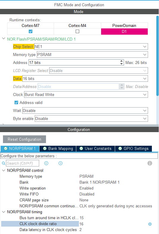
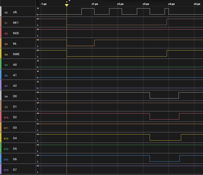
I am trying to get the FMC to work in 16-bit synchronous mode but I only get an output with 4 clocks (64-bit) instead.
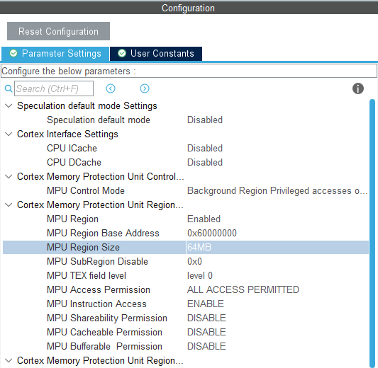
In other threads [1], [2] I found that I should either switch the address from 0x60000000 to 0xC0000000 or enable the MPU, but neither approach works for me.
This is my config:
FMC:
MPU:
Usage:
uint16_t * psram16 = (uint16_t *)0x60000000;
psram16[0] = 0x00AA;
Output:
What am I missing?
- Labels:
-
FMC-FSMC
-
STM32H7 Series
- Mark as New
- Bookmark
- Subscribe
- Mute
- Subscribe to RSS Feed
- Permalink
- Email to a Friend
- Report Inappropriate Content
2023-12-08 12:06 AM - edited 2023-12-08 12:07 AM
Hello @Kurngop32 and welcome to the Community :),
According to RM0399, for some PSRAM memories which must be configured to Synchronous mode, during the
BCR register writing, the memory attribute space must be configured to device or strongly-ordered. Once PSRAM BCR register is configured, the memory attribute of PSRAM address space can be programmed to cacheable.
Could you please check these settings?
Thank you.
Kaouthar
To give better visibility on the answered topics, please click on Accept as Solution on the reply which solved your issue or answered your question.
- Mark as New
- Bookmark
- Subscribe
- Mute
- Subscribe to RSS Feed
- Permalink
- Email to a Friend
- Report Inappropriate Content
2023-12-08 04:26 AM
Not sure what this means. Isn't that the MPU setting?
I also tried it without CubeMX:
MPU->CTRL = 0;
MPU->RBAR = (0x60000000 & MPU_RBAR_ADDR_Msk)
	| (1 << MPU_RBAR_VALID_Pos)
	| (0 << MPU_RBAR_REGION_Pos);
MPU->RASR = (1 << MPU_RASR_XN_Pos)		// execute never
	| (0b011 << MPU_RASR_AP_Pos)  		// access: full
	| (0b000 << MPU_RASR_TEX_Pos)		// type extension
	| (1 << MPU_RASR_S_Pos)			// sharable
	| (0 << MPU_RASR_C_Pos)			// cacheable
	| (0 << MPU_RASR_B_Pos)			// bufferable
	| (0 << MPU_RASR_SRD_Pos) 		// subregion
	| (MPU_REGION_SIZE_128KB << MPU_RASR_SIZE_Pos) 	// size: 2^(val+1)
	| (1 << MPU_RASR_ENABLE_Pos);
MPU->CTRL = MPU_CTRL_PRIVDEFENA_Msk | MPU_CTRL_ENABLE_Msk;
- Mark as New
- Bookmark
- Subscribe
- Mute
- Subscribe to RSS Feed
- Permalink
- Email to a Friend
- Report Inappropriate Content
2023-12-08 05:43 AM
Hi @Kurngop32 ,
Yes, I mean that the memory region MPU attribute must be configured as “Device" or “strongly-ordered".
I think that FMC_PSRAM example can help you. This example describes how to configure the FMC controller to access the PSRAM memory. The PSRAM is IS66WV51216EBLL-55BLI. This example has been tested with STM32F723E-Discovery board and can be easily tailored to any other device and development board.
I hope this help you!
Kaouthar
To give better visibility on the answered topics, please click on Accept as Solution on the reply which solved your issue or answered your question.
- Mark as New
- Bookmark
- Subscribe
- Mute
- Subscribe to RSS Feed
- Permalink
- Email to a Friend
- Report Inappropriate Content
2023-12-08 06:54 AM
This leaves more questions than it answers. In the example, additionally to what I already did, another memory region at 0xA0000000 is created, no idea why since this is reserved space, but it does not help anyway. To be sure I set the whole memory to strongly-ordered, but that does not change anything. The output looks still the same, i.e. 4 clocks instead of 1.
- Mark as New
- Bookmark
- Subscribe
- Mute
- Subscribe to RSS Feed
- Permalink
- Email to a Friend
- Report Inappropriate Content
2023-12-08 07:14 AM - edited 2023-12-08 07:15 AM
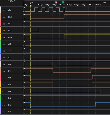
btw this is how a 32 bit access looks:
uint32_t * psram32 = (uint32_t *)0x60000000;
psram32[0] = 0x00A000A1;
5 clocks, so also 3 unnecessary clocks (or my expectation is wrong, I don’t have much experience with external memories)
- Mark as New
- Bookmark
- Subscribe
- Mute
- Subscribe to RSS Feed
- Permalink
- Email to a Friend
- Report Inappropriate Content
2023-12-18 08:13 AM
Hello @Kurngop32 ,
Do you see the same behavior when using DMA?
To check this issue, could you please share your project?
Thanks and best regards,
Kaouthar
To give better visibility on the answered topics, please click on Accept as Solution on the reply which solved your issue or answered your question.
- Mark as New
- Bookmark
- Subscribe
- Mute
- Subscribe to RSS Feed
- Permalink
- Email to a Friend
- Report Inappropriate Content
2023-12-20 01:58 AM
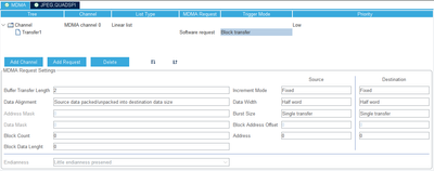
No difference with MDMA.
uint16_t src=0x1234;
HAL_MDMA_Start(&hmdma_mdma_channel0_sw_0, (uint32_t)&src, 0x60000000, 2, 1);
You can make a new project (STM32H745XIH6, FW H7 1.11.1), with the settings from the first post. I didn't change or configure anything else.
FMC is accessed right before the main while loop.
- Mark as New
- Bookmark
- Subscribe
- Mute
- Subscribe to RSS Feed
- Permalink
- Email to a Friend
- Report Inappropriate Content
2024-08-29 03:04 AM
I'm still trying to solve this issue.
for reference here again my latest try:
  uint16_t * psram16 = (uint16_t *)0x60000000;
  //   080013A2   F04F 43C0   MOV.W          R3, #0x60000000
  //   080013A6   607B        STR            R3, [R7, #4]
  psram16[0] = 0x0005;
  //   080013A8   687B        LDR            R3, [R7, #4]
  //   080013AA   2205        MOVS           R2, #5
  //   080013AC   801A        STRH           R2, [R3]
From what I understand, this should be a 16-bit access on the AXI and FMC should not output 4 clocks
Can anyone confirm, that it is possible to output only a single clock write/read access with 16-bit data width?
- Issue Interfacing Winbond W25Q16JV with STM32H745 Custom Board (QSPI) in STM32 MCUs Boards and hardware tools
- STLINK-V3MINIE not detected in debug mode in STM32 MCUs Boards and hardware tools
- stm32h745 dual core run configuration in STM32CubeIDE (MCUs)
- mbedtls vs wolfssl in STM32 MCUs Embedded software
- Facing issues with integration of low volume pendrive with STM32H747 Board in STM32 MCUs Embedded software
