- STMicroelectronics Community
- STM32 MCUs
- STM32 MCUs Products
- Re: STM32G031 TIM2 PWM Mode 1 using DMA generating...
- Subscribe to RSS Feed
- Mark Topic as New
- Mark Topic as Read
- Float this Topic for Current User
- Bookmark
- Subscribe
- Mute
- Printer Friendly Page
STM32G031 TIM2 PWM Mode 1 using DMA generating odd waveforms
- Mark as New
- Bookmark
- Subscribe
- Mute
- Subscribe to RSS Feed
- Permalink
- Email to a Friend
- Report Inappropriate Content
2019-12-12 04:40 AM
We're porting some existing working code to the STM32G031J6M6.
On pin 5, we are using TIM3CH3, and passing high time data from an 8 bit array to the 16 bit CCR3 register, and the waveform is as expected - correct.
On pin 4, we are using TIM2CH1, and passing high time data from the same 8 bit array to the 32 bit CCR1 register, and the waveform has the correct high time mixed in with one other pulse of variable length, and a much longer than expected period.
Is there any known issue with using TIM2CH1 for PWM Mode 1 on this device?
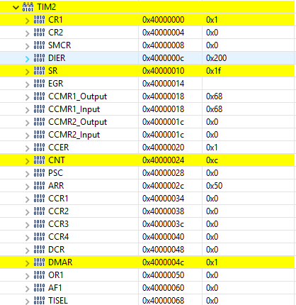
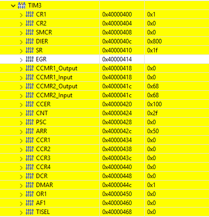
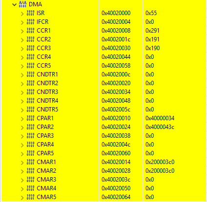
The SFRs for DMA, TIM2 and TIM3 are shown below.
- Labels:
-
DMA
-
STM32G0 Series
-
TIM
- Mark as New
- Bookmark
- Subscribe
- Mute
- Subscribe to RSS Feed
- Permalink
- Email to a Friend
- Report Inappropriate Content
2019-12-12 06:56 PM
Registers look OK to me.
Can't the problem be in how DMAMUX is configured?
JW
- Mark as New
- Bookmark
- Subscribe
- Mute
- Subscribe to RSS Feed
- Permalink
- Email to a Friend
- Report Inappropriate Content
2019-12-13 06:56 AM
Thanks for the reply.
I took a look at the DMAMUX, and ruled it out by writing a loop that updated the CCR1 register when the channel 1 flag was set in the SR. The result is the same.
The reaction looks as if the CNT register is sometimes not resetting at ARR, but is running to maximum and wrapping, then I get an edge on the next match with CCR1. Very odd.
- Mark as New
- Bookmark
- Subscribe
- Mute
- Subscribe to RSS Feed
- Permalink
- Email to a Friend
- Report Inappropriate Content
2019-12-14 12:33 AM
> as if the CNT register is sometimes not resetting at ARR, but is running to maximum
Would that be the case, given TIM2 is 32-bit, that would take time in the order of 100 seconds (i.e. a couple of minutes). You should be able to observe that by repeatedly reading out the TIM regsiters' content in debugger.
Try reducing the program to bare minimum, and post it here with together with observed waveform and explain how exactly is it different from the expectation.
Also, as you are using the SO8 package i.e. where several pads are bonded together to one pin, don't you have a conflict on the given pin with other port pad? Check in the GPIO registers. Do you use an oscilloscope or a LA to observe the port pin? Don't you have conflict with the debugger?
JW
- Mark as New
- Bookmark
- Subscribe
- Mute
- Subscribe to RSS Feed
- Permalink
- Email to a Friend
- Report Inappropriate Content
2019-12-16 01:35 AM
Thanks for the reply.
The code that we used for TIM2CH1 was a tight loop, polling the registers (the execution time of the standard STM drivers is too long in this instance)
In the end, we have removed the TIM2CH1 code and used TIM3CH3 and TIM3CH2. TIM3CH2 is on pin8 of the device, which is why we avoided it originally, as it is assigned to SWCLK (luckily, we can work with testing most elements on TIM3CH3 only, leaving the part to run on TIM3CH2 also when it is off the debugger). On this channel, we are using DMA Ch1, and it generates the waveform below.
The GPIO settings that we used for Pin 4 appeared to be correct (in fact, we went through all of the other potential users of the pin in the debugger to rule them out).
We're perfectly prepared to accept that we have done something wrong with TIM2CH1 on the microprocessor, but we use quite a number of other STM processors and TIM1, 2, 8 etc in PWM mode 1 with no issues, it appears to be related to this device.
We'll return to the problem when we have more time, but if anyone has an example of this device working correctly on TIM2CH1, then please post the code.
- Cannot set deadtime for HRTIM1 in NUCLEO-G474 in STM32 MCUs Products
- Dual waveform generation on DACs of NUCLEO H7A3ZI-Q in STM32 MCUs Boards and hardware tools
- STM32H5 Waveform Generation using External DAC in STM32 MCUs Products
- Using the DMABurst feature to generate an abitrary waveform in STM32 MCUs Products
- AN4776 STM32f303 Swap Tim1 and Tim2 N-pulse waveform generation application example - part 1 in STM32 MCUs Embedded software


