- STMicroelectronics Community
- STM32 MCUs
- STM32 MCUs Products
- Re: STM32F7 and Extern SDRAM Bank Accessing Proble...
- Subscribe to RSS Feed
- Mark Topic as New
- Mark Topic as Read
- Float this Topic for Current User
- Bookmark
- Subscribe
- Mute
- Printer Friendly Page
STM32F7 and Extern SDRAM Bank Accessing Problem
- Mark as New
- Bookmark
- Subscribe
- Mute
- Subscribe to RSS Feed
- Permalink
- Email to a Friend
- Report Inappropriate Content
2019-04-03 07:22 AM
Hi everyone,
I'm using a STM32F769BGT6 with an external SDRAM (IS42S32400F). This SDRAM is composed of 4 banks. Each bank contains 12 Rows (4096), 8 Columns (256), and each cell is 32 bits. So : 4096*256*32 = 33 554 432 bits, or 4MBytes/Bank. That means that it can store 4x1M uint32 variables.
I've done the configuration in system_stm32f7xx.c, because i need to use it as a memory section. Here is the initialization code :
void SystemInit_ExtMemCtl(void)
{
  __IO uint32_t tmp = 0;

  register uint32_t tmpreg = 0, timeout = 0xFFFF;
  register uint32_t index;

  /* Enable GPIOD, GPIOE, GPIOF, GPIOG, GPIOH and GPIOI interface clock */
  RCC->AHB1ENR |= 0x000001F8;

  /* Delay after an RCC peripheral clock enabling */
  tmp = READ_BIT(RCC->AHB1ENR, RCC_AHB1ENR_GPIOEEN);

  /* Connect PDx pins to FMC Alternate function */
  GPIOD->AFR[0]  = 0x000000CC;
  GPIOD->AFR[1]  = 0xCC000CCC;
  /* Configure PDx pins in Alternate function mode */
  GPIOD->MODER   = 0xA02A000A;
  /* Configure PDx pins speed to 100 MHz */
  GPIOD->OSPEEDR = 0xF03F000F;
  /* Configure PDx pins Output type to push-pull */
  GPIOD->OTYPER  = 0x00000000;
  /* No pull-up, pull-down for PDx pins */
  GPIOD->PUPDR   = 0x50150005;

  /* Connect PEx pins to FMC Alternate function */
  GPIOE->AFR[0]  = 0xC00000CC;
  GPIOE->AFR[1]  = 0xCCCCCCCC;
  /* Configure PEx pins in Alternate function mode */
  GPIOE->MODER   = 0xAAAA800A;
  /* Configure PEx pins speed to 100 MHz */
  GPIOE->OSPEEDR = 0xFFFFC00F;
  /* Configure PEx pins Output type to push-pull */
  GPIOE->OTYPER  = 0x00000000;
  /* No pull-up, pull-down for PEx pins */
  GPIOE->PUPDR   = 0x55554005;

  /* Connect PFx pins to FMC Alternate function */
  GPIOF->AFR[0]  = 0x00CCCCCC;
  GPIOF->AFR[1]  = 0xCCCCC000;
  /* Configure PFx pins in Alternate function mode */
  GPIOF->MODER   = 0xAA800AAA;
  /* Configure PFx pins speed to 100 MHz */
  GPIOF->OSPEEDR = 0xFFC00FFF;
  /* Configure PFx pins Output type to push-pull */
  GPIOF->OTYPER  = 0x00000000;
  /* No pull-up, pull-down for PFx pins */
  GPIOF->PUPDR   = 0x55400555;

  /* Connect PGx pins to FMC Alternate function */
  GPIOG->AFR[0]  = 0x00CC00CC;
  GPIOG->AFR[1]  = 0xC000000C;
  /* Configure PGx pins in Alternate function mode */
  GPIOG->MODER   = 0x80020A0A;
  /* Configure PGx pins speed to 100 MHz */
  GPIOG->OSPEEDR = 0xC0030F0F;
  /* Configure PGx pins Output type to push-pull */
  GPIOG->OTYPER  = 0x00000000;
  /* No pull-up, pull-down for PGx pins */
  GPIOG->PUPDR   = 0x40010505;

  /* Connect PHx pins to FMC Alternate function */
  GPIOH->AFR[0]  = 0x00C0CC00;
  GPIOH->AFR[1]  = 0xCCCCCCCC;
  /* Configure PHx pins in Alternate function mode */
  GPIOH->MODER   = 0xAAAA08A0;
  /* Configure PHx pins speed to 100 MHz */
  GPIOH->OSPEEDR = 0xFFFF0CF0;
  /* Configure PHx pins Output type to push-pull */
  GPIOH->OTYPER  = 0x00000000;
  /* No pull-up, pull-down for PHx pins */
  GPIOH->PUPDR   = 0x55550450;

  /* Connect PIx pins to FMC Alternate function */
  GPIOI->AFR[0]  = 0xCCCCCCCC;
  GPIOI->AFR[1]  = 0x00000CC0;
  /* Configure PIx pins in Alternate function mode */
  GPIOI->MODER   = 0x0028AAAA;
  /* Configure PIx pins speed to 100 MHz */
  GPIOI->OSPEEDR = 0x003CFFFF;
  /* Configure PIx pins Output type to push-pull */
  GPIOI->OTYPER  = 0x00000000;
  /* No pull-up, pull-down for PIx pins */
  GPIOI->PUPDR   = 0x00145555;

/*-- FMC Configuration ------------------------------------------------------*/
  /* Enable the FMC interface clock */
  RCC->AHB3ENR |= 0x00000001;
  // FMC_Bank5_6->MWID = 0x
  /* Delay after an RCC peripheral clock enabling */
  tmp = READ_BIT(RCC->AHB3ENR, RCC_AHB3ENR_FMCEN);

  /* Configure and enable SDRAM bank1 */
  FMC_Bank5_6->SDCR[0] = 0x00001BE4;
  FMC_Bank5_6->SDTR[0] = 0x01115361;

  /* SDRAM initialization sequence */
  /* Clock enable command */
  FMC_Bank5_6->SDCMR = 0x00000011;
  tmpreg = FMC_Bank5_6->SDSR & 0x00000020;
  while((tmpreg != 0) && (timeout-- > 0))
  {
    tmpreg = FMC_Bank5_6->SDSR & 0x00000020;
  }

  /* Delay */
  for (index = 0; index<1000; index++);

  /* PALL command */
  FMC_Bank5_6->SDCMR = 0x00000012;
  timeout = 0xFFFF;
  while((tmpreg != 0) && (timeout-- > 0))
  {
    tmpreg = FMC_Bank5_6->SDSR & 0x00000020;
  }

  /* Auto refresh command */
  FMC_Bank5_6->SDCMR = 0x000000F3;
  timeout = 0xFFFF;
  while((tmpreg != 0) && (timeout-- > 0))
  {
    tmpreg = FMC_Bank5_6->SDSR & 0x00000020;
  }

  /* MRD register program */
  FMC_Bank5_6->SDCMR = 0x00046014;
  timeout = 0xFFFF;
  while((tmpreg != 0) && (timeout-- > 0))
  {
    tmpreg = FMC_Bank5_6->SDSR & 0x00000020;
  }

  /* Set refresh count */
  tmpreg = FMC_Bank5_6->SDRTR;
  FMC_Bank5_6->SDRTR = (tmpreg | (0x00000603<<1));

  /* Disable write protection */
  tmpreg = FMC_Bank5_6->SDCR[0];
  FMC_Bank5_6->SDCR[0] = (tmpreg & 0xFFFFFDFF);

  /*
   * Disable the FMC bank1 (enabled after reset).
   * This, prevents CPU speculation access on this bank which blocks the use of FMC during
   * 24us. During this time the others FMC master (such as LTDC) cannot use it!
   */
  FMC_Bank1->BTCR[0] = 0x000030d2;

  (void)(tmp);
}
On line 94 of this code snippet, you can see this value for SDCR register :
FMC_Bank5_6->SDCR[0] = 0x00001BE4;
The "B" means that I chose a Memory Data Bus Width of 32 bits.
I made a modification in the linker to add a memory section like follows :
/* Specify the memory areas */
MEMORY
{
RAM (xrw)       : ORIGIN = 0x20000000, LENGTH = 512K
FLASH (rx)      : ORIGIN = 0x08000000, LENGTH = 1024K
SDRAM (xrw)     : ORIGIN = 0xC0000000, LENGTH = 16M
}

/* Define output sections */
SECTIONS
{
  /* Section créée pour l'allocation dans la SDRAM externe*/
  .masection :
  {
    . = ALIGN(4);
    *(.masection)
    *(.masection*)
    . = ALIGN(4);
  } >SDRAM
The following code, in the main.c, tests that I can write in the entire memory :
const uint32_t testSize2 = 4000000;

uint32_t volatile memoryTest2[testSize2] __attribute__((section(".masection")));

  for(size_t i = 0; i < testSize2; i++)
  {
    memoryTest2[i] = i;
  }

  for(size_t i = 0; i < testSize2; i++)
  {
    if(memoryTest2[i] != i) __DEBUG_BKPT();
  }
It creates a tab of 4M uint32, and works perfectly.
Sorry for the long intro, but I wanted this to be very clear for you and for myself.
Now my question is :
I need to use a Memory Data Bus Width of 8 bits, instead of 32, because I will use this memory section exclusively with 8 bits words.
For this, I simply changed FMC_Bank5_6->SDCR[0] = 0x00001CE4;
Now, I cannot create a tab of 4M uint32t anymore, I'm limited to 1M. If I try to add more, I have a hardfault. I have the feeling that the low level FMC drivers are not dealing with 8 bits data width properly.
This is very frustrating because 1/4 of my memory is not accessible and I'm stuck.
If anyone has an idea on this, it would be great!
Thanks for your time.
- Labels:
-
FMC-FSMC
-
STM32F7 Series
- Mark as New
- Bookmark
- Subscribe
- Mute
- Subscribe to RSS Feed
- Permalink
- Email to a Friend
- Report Inappropriate Content
2019-04-03 04:37 PM
>>I need to use a Memory Data Bus Width of 8 bits, instead of 32, because I will use this memory section exclusively with 8 bits words.
WHY?
Doesn't the interface support BYTE LANES?
>> If I try to add more, I have a hardfault.
Yeah, no kidding. The memory region is constrained via rows/columns/width, it is like the old 68000, it faults if you access non-existent memory.
Up vote any posts that you find helpful, it shows what's working..
- Mark as New
- Bookmark
- Subscribe
- Mute
- Subscribe to RSS Feed
- Permalink
- Email to a Friend
- Report Inappropriate Content
2019-04-04 07:42 AM
Hi Clive,
Thanks for the answer.
I figured a few things out reading this post : https://community.st.com/s/question/0D50X00009XkYQCSA3/stm32f407-fsmc-physical-addressing
I noticed two things by re-reading the RM :
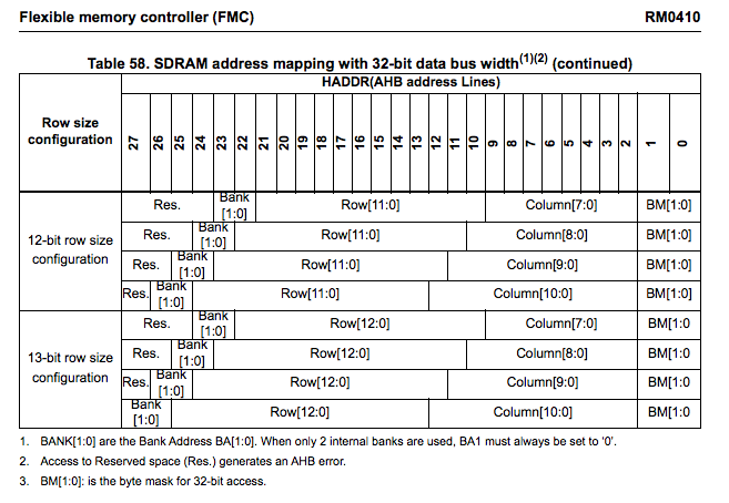
Here I see that BM[1:0] is a byte mask for 32-bit access.
And here :
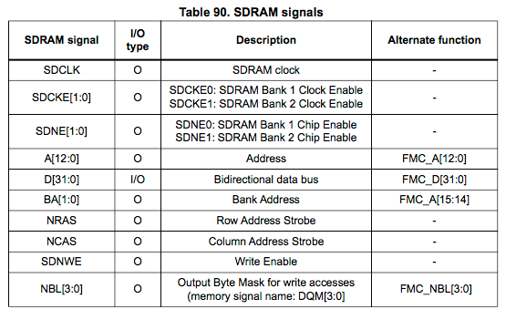
FMC_NBL[3:0] Seems to be related to my issue as well.
I can't figure out what you mean by BYTE LANES. I assume it is related with what is above. Could you enlighten me a little more?
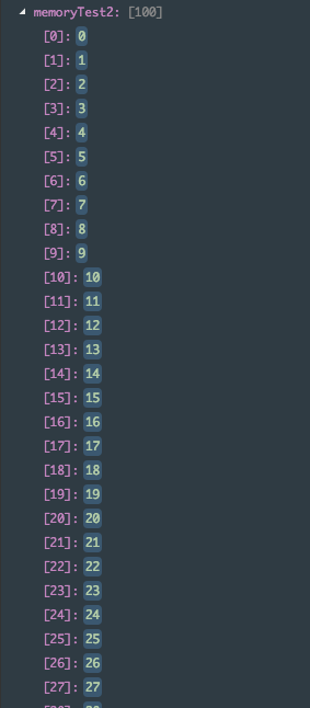
Here is what I get when I try to write UINT32 elements in SDRAM set to 32b width (Code in my previous post) :
As you can see, everything's fine.
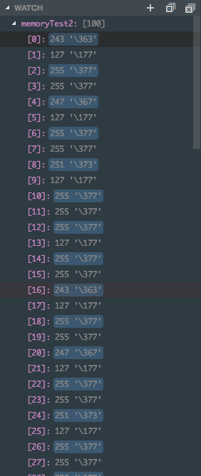
Now here is the result for a uint8 tab :
As always, thanks for your time.
- Mark as New
- Bookmark
- Subscribe
- Mute
- Subscribe to RSS Feed
- Permalink
- Email to a Friend
- Report Inappropriate Content
2019-04-04 08:07 AM
>>I can't figure out what you mean by BYTE LANES. I assume it is related with what is above. Could you enlighten me a little more?
32-bit wide memories are managed by the bus controller and CPU, where a barrel shifter gets bytes written to memory in the right position across the 32-bit word, and then instructs the memory to take specific byte(s) from the presented data. This is also used with you have unaligned 32-bit writes that span two different 32-bit memory locations. ie (addr & 3) != 0
http://infocenter.arm.com/help/index.jsp?topic=/com.arm.doc.ddi0203f/I1044275.html
Is this a custom board constructed yourself? What is the pinning?
I would go with a 50 MHz "speed" settings, the slew rate here is a bit aggressive for short traces without series resistors.
Up vote any posts that you find helpful, it shows what's working..
- Mark as New
- Bookmark
- Subscribe
- Mute
- Subscribe to RSS Feed
- Permalink
- Email to a Friend
- Report Inappropriate Content
2019-04-04 08:12 AM
Do i need to do something specific to have those BYTE LANES pins NBL[3:0] to properly mask data when I try to write bytes? I assume it is handled by the FMC, but maybe I have to use exclusively HAL methods to have it working?
- Mark as New
- Bookmark
- Subscribe
- Mute
- Subscribe to RSS Feed
- Permalink
- Email to a Friend
- Report Inappropriate Content
2019-04-04 08:35 AM
Post initialization the HAL plays no role, it is a configure and forget set up. You have to setup the pins, controller and memory correctly from the outset.
I'm not going to dig through register level code to validate it. My approach would be to use the verbose HAL configuration methods and examples first, and validate the read/write functionality of the SDRAM array at 8, 16 and 32-bit widths. Once that's done I'd migrate to the register level stuff. In the past I've had to do this for a number of DISCO boards because ST only provided code for the EVAL boards.
Up vote any posts that you find helpful, it shows what's working..
- Mark as New
- Bookmark
- Subscribe
- Mute
- Subscribe to RSS Feed
- Permalink
- Email to a Friend
- Report Inappropriate Content
2019-04-04 08:46 AM
Thanks for the link, much clearer now.
The board is custom yes.
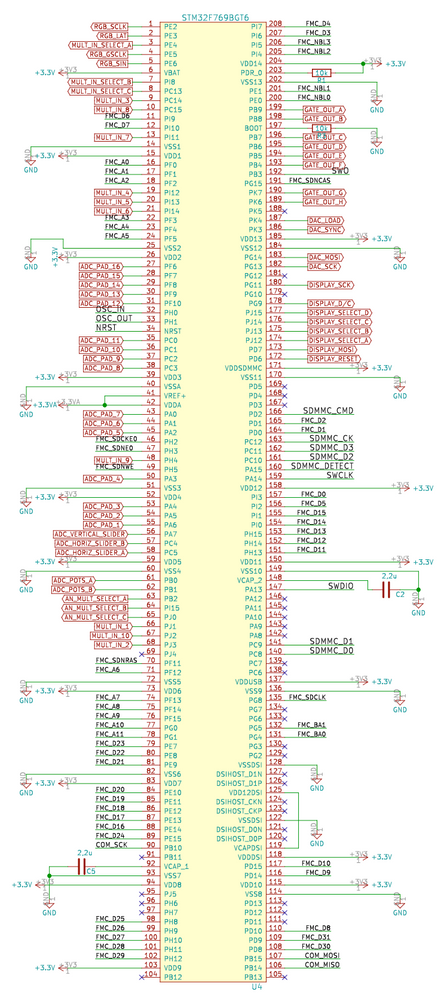
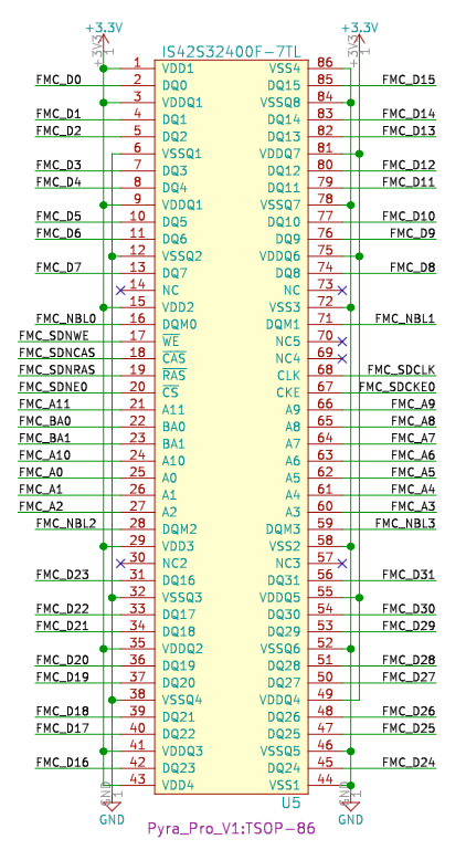
Here is the pinout :
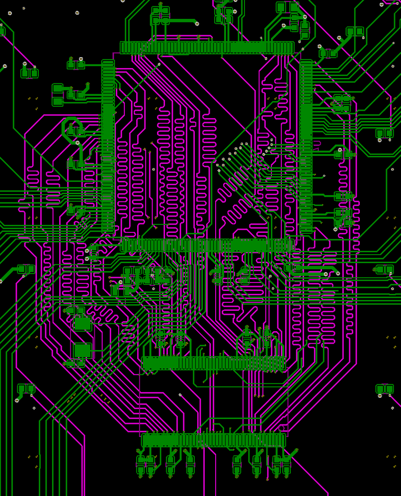
And here is what the length matched traces look like:
- Mark as New
- Bookmark
- Subscribe
- Mute
- Subscribe to RSS Feed
- Permalink
- Email to a Friend
- Report Inappropriate Content
2019-04-04 08:48 AM
I set SDCLK to the minimum (3xHCLK periods) and CAS latency to the max to avoid timing problems but results in my tab are the same than before.
- Mark as New
- Bookmark
- Subscribe
- Mute
- Subscribe to RSS Feed
- Permalink
- Email to a Friend
- Report Inappropriate Content
2019-04-04 09:59 AM
The pin diagrams here are unreadably small/low-res
Test your memory read/write 32/8-bit code on an STM32F769I-DISCO, see that they work properly there, where the width is managed transparently.
Create your own long-hand form of the HAL's BSP SDRAM code like that for the DISCO, but for your own board. STM32Cube_FW_F7_V1.15.0\Drivers\BSP\STM32F769I-Discovery\stm32f769i_discovery_sdram.c
All the SDRAM settings need to be coherent across the controller, and SDRAM configuration writes.
Set aside your desire to get the SDRAM working at startup, and validate it first using the later stage HAL method.
Up vote any posts that you find helpful, it shows what's working..
- Mark as New
- Bookmark
- Subscribe
- Mute
- Subscribe to RSS Feed
- Permalink
- Email to a Friend
- Report Inappropriate Content
2019-04-04 10:01 AM
Suggests a more pin level issue. Figure several hours of work to unravel
Up vote any posts that you find helpful, it shows what's working..
- STM32F7 - USB problems on Windows - SMT32Cube FW_F7 V.1.17.2 broken? in STM32 MCUs Products
- STM32F103C8T6 Firmware for Bootloader in STM32 MCUs Products
- Pin sharing problem with SWD and SPI3, GPIO in STM32 MCUs Wireless
- Problem in STM32F7 with ethernetif.c provided by STM32CubeIDE 1.7.0 in STM32 MCUs Embedded software
- SPI SSD1306 and I2C MPU6050 on stm32f103c8t6 in STM32 MCUs Boards and hardware tools
