- STMicroelectronics Community
- STM32 MCUs
- STM32 MCUs Products
- STM32F405 - Backup SRAM not preserved
- Subscribe to RSS Feed
- Mark Topic as New
- Mark Topic as Read
- Float this Topic for Current User
- Bookmark
- Subscribe
- Mute
- Printer Friendly Page
STM32F405 - Backup SRAM not preserved
- Mark as New
- Bookmark
- Subscribe
- Mute
- Subscribe to RSS Feed
- Permalink
- Email to a Friend
- Report Inappropriate Content
2023-09-20 6:20 PM - edited 2023-09-20 6:22 PM
I have a STM32F405 with a coin cell on VBAT and I haven't been able to get the Backup SRAM or RTC to preserve contents when removing main power. The same code works fine on another board that has a STM32F407.
//Works on STM32F407 - Fails on STM32F405

backup_SRAM_data_t* backup_SRAM_data_ptr = (backup_SRAM_data_t*)BKPSRAM_BASE;

//Enable backup SRAM
__HAL_RCC_BKPSRAM_CLK_ENABLE();
HAL_PWR_EnableBkUpAccess();
HAL_PWREx_EnableBkUpReg();

printf("[%u] Read = %u\n", (unsigned int)HAL_GetTick(), (unsigned int)backup_SRAM_data_ptr->test_var);
backup_SRAM_data_ptr->test_var = 7;
printf("[%u] Write = %u\n", (unsigned int)HAL_GetTick(), (unsigned int)backup_SRAM_data_ptr->test_var);
printf("[%u] Read = %u\n", (unsigned int)HAL_GetTick(), (unsigned int)backup_SRAM_data_ptr->test_var);
Adding an enable of the PWR clock doesn't fix it - that's already done in SystemClock_Config(), which is called earlier in the code.
//Still fails on STM32F405

//Enable backup SRAM
__HAL_RCC_PWR_CLK_ENABLE();       //Enable PWR clock
HAL_PWR_EnableBkUpAccess();       //Enable access to backup domain
__HAL_RCC_BKPSRAM_CLK_ENABLE();   //Enable backup SRAM clock
HAL_PWREx_EnableBkUpReg();        //Enable backup SRAM low power regulator
A 3V (~3.3V fully charged) coin cell is directly connected to the VBAT pin. The STM32F405 is the 64-pin package, so there's no PDR_ON pin. The working STM32F407 is the 100 pin package. There's an external 32.768kHz XTL and LSE is enabled. The only obvious difference between the two boards is that the working F407 has a 25MHz XTL used for HSE and the F405 uses the internal 16MHz HSI.
Any thoughts on why VBAT isn't preserving SRAM? Please let me know if there's any additional info or debugging steps I can provide that would be useful.
//Autogenerated by CubeMX - STM32F405

void SystemClock_Config(void)
{
  RCC_OscInitTypeDef RCC_OscInitStruct = {0};
  RCC_ClkInitTypeDef RCC_ClkInitStruct = {0};

  /** Configure the main internal regulator output voltage
  */
  __HAL_RCC_PWR_CLK_ENABLE();
  __HAL_PWR_VOLTAGESCALING_CONFIG(PWR_REGULATOR_VOLTAGE_SCALE1);

  /** Initializes the RCC Oscillators according to the specified parameters
  * in the RCC_OscInitTypeDef structure.
  */
  RCC_OscInitStruct.OscillatorType = RCC_OSCILLATORTYPE_HSI|RCC_OSCILLATORTYPE_LSI
                              |RCC_OSCILLATORTYPE_LSE;
  RCC_OscInitStruct.LSEState = RCC_LSE_ON;
  RCC_OscInitStruct.HSIState = RCC_HSI_ON;
  RCC_OscInitStruct.HSICalibrationValue = RCC_HSICALIBRATION_DEFAULT;
  RCC_OscInitStruct.LSIState = RCC_LSI_ON;
  RCC_OscInitStruct.PLL.PLLState = RCC_PLL_ON;
  RCC_OscInitStruct.PLL.PLLSource = RCC_PLLSOURCE_HSI;
  RCC_OscInitStruct.PLL.PLLM = 16;
  RCC_OscInitStruct.PLL.PLLN = 128;
  RCC_OscInitStruct.PLL.PLLP = RCC_PLLP_DIV2;
  RCC_OscInitStruct.PLL.PLLQ = 4;
  if (HAL_RCC_OscConfig(&RCC_OscInitStruct) != HAL_OK)
  {
    Error_Handler();
  }

  /** Initializes the CPU, AHB and APB buses clocks
  */
  RCC_ClkInitStruct.ClockType = RCC_CLOCKTYPE_HCLK|RCC_CLOCKTYPE_SYSCLK
                              |RCC_CLOCKTYPE_PCLK1|RCC_CLOCKTYPE_PCLK2;
  RCC_ClkInitStruct.SYSCLKSource = RCC_SYSCLKSOURCE_PLLCLK;
  RCC_ClkInitStruct.AHBCLKDivider = RCC_SYSCLK_DIV1;
  RCC_ClkInitStruct.APB1CLKDivider = RCC_HCLK_DIV2;
  RCC_ClkInitStruct.APB2CLKDivider = RCC_HCLK_DIV1;

  if (HAL_RCC_ClockConfig(&RCC_ClkInitStruct, FLASH_LATENCY_2) != HAL_OK)
  {
    Error_Handler();
  }
}
//Auto-generated by CubeMX - STM32F407
void SystemClock_Config(void)
{
RCC_OscInitTypeDef RCC_OscInitStruct = {0};
RCC_ClkInitTypeDef RCC_ClkInitStruct = {0};
/** Configure the main internal regulator output voltage
*/
__HAL_RCC_PWR_CLK_ENABLE();
__HAL_PWR_VOLTAGESCALING_CONFIG(PWR_REGULATOR_VOLTAGE_SCALE1);
/** Initializes the RCC Oscillators according to the specified parameters
* in the RCC_OscInitTypeDef structure.
*/
RCC_OscInitStruct.OscillatorType = RCC_OSCILLATORTYPE_LSI|RCC_OSCILLATORTYPE_HSE
|RCC_OSCILLATORTYPE_LSE;
RCC_OscInitStruct.HSEState = RCC_HSE_ON;
RCC_OscInitStruct.LSEState = RCC_LSE_ON;
RCC_OscInitStruct.LSIState = RCC_LSI_ON;
RCC_OscInitStruct.PLL.PLLState = RCC_PLL_ON;
RCC_OscInitStruct.PLL.PLLSource = RCC_PLLSOURCE_HSE;
RCC_OscInitStruct.PLL.PLLM = 25;
RCC_OscInitStruct.PLL.PLLN = 320;
RCC_OscInitStruct.PLL.PLLP = RCC_PLLP_DIV2;
RCC_OscInitStruct.PLL.PLLQ = 4;
if (HAL_RCC_OscConfig(&RCC_OscInitStruct) != HAL_OK)
{
Error_Handler();
}
/** Initializes the CPU, AHB and APB buses clocks
*/
RCC_ClkInitStruct.ClockType = RCC_CLOCKTYPE_HCLK|RCC_CLOCKTYPE_SYSCLK
|RCC_CLOCKTYPE_PCLK1|RCC_CLOCKTYPE_PCLK2;
RCC_ClkInitStruct.SYSCLKSource = RCC_SYSCLKSOURCE_PLLCLK;
RCC_ClkInitStruct.AHBCLKDivider = RCC_SYSCLK_DIV1;
RCC_ClkInitStruct.APB1CLKDivider = RCC_HCLK_DIV8;
RCC_ClkInitStruct.APB2CLKDivider = RCC_HCLK_DIV2;
if (HAL_RCC_ClockConfig(&RCC_ClkInitStruct, FLASH_LATENCY_5) != HAL_OK)
{
Error_Handler();
}
}
Solved! Go to Solution.
- Labels:
-
RAM
-
RCC
-
STM32F4 Series
Accepted Solutions
- Mark as New
- Bookmark
- Subscribe
- Mute
- Subscribe to RSS Feed
- Permalink
- Email to a Friend
- Report Inappropriate Content
2023-09-22 3:09 PM - edited 2023-09-22 3:12 PM
Pins 18/19 are VSS/VDD pair, but nonetheless:
[Can't upload image due to Khoros/ST limiting number of images I can upload... Sigh.]
STM32F405/407 datasheet, Power supply schemes chapter: VDDA and VSSA must be connected to VDD and VSS , respectively.
Power supply scheme, footnote: VDDA = VSSA.
Absolute maximum ratings, Variations between different VDD power pins, max. 50mV.
The 0.3V difference in your case is probably not detrimental to actual operation when VDD/VDDA are up, but, the current spike you've described above... have you read the story I've linked to? As reset circuitry which also switches over from VBAT to VDD for the backup-power domain is controlled from VDDA, if VDDA rises later than VDD, the whole mcu is powered from VBAT during that moment.
JW
- Mark as New
- Bookmark
- Subscribe
- Mute
- Subscribe to RSS Feed
- Permalink
- Email to a Friend
- Report Inappropriate Content
2023-09-20 7:50 PM
Is it being preserved on reset? If not, could be getting cleared during initialization.
- Mark as New
- Bookmark
- Subscribe
- Mute
- Subscribe to RSS Feed
- Permalink
- Email to a Friend
- Report Inappropriate Content
2023-09-20 9:34 PM - edited 2023-09-21 12:03 AM
Verify (physically, think bad solder joints) that all VDD and ground pins are connected, including the analog ones, also PDR_ON if present in given package, and VBAT itself.
Check by reading out PWR_CSR that the backup power regulator is enabled.
JW
- Mark as New
- Bookmark
- Subscribe
- Mute
- Subscribe to RSS Feed
- Permalink
- Email to a Friend
- Report Inappropriate Content
2023-09-21 1:10 AM
Try measuring the current from the battery when the main power is off. If it is significantly less than the MCU that works, there is probably a faulty MCU or a PCB or soldering problem.
- Mark as New
- Bookmark
- Subscribe
- Mute
- Subscribe to RSS Feed
- Permalink
- Email to a Friend
- Report Inappropriate Content
2023-09-22 9:35 AM - edited 2023-09-22 10:41 AM
@TDK - Yes, the data is preserved across resets as long as VDD stays at 3.3V.
- Mark as New
- Bookmark
- Subscribe
- Mute
- Subscribe to RSS Feed
- Permalink
- Email to a Friend
- Report Inappropriate Content
2023-09-22 2:42 PM - edited 2023-09-22 2:46 PM
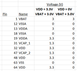
@waclawek.jan - All the power pins are connected, the following table shows voltages measured on MCU pins with w/ and w/o VDD active. All VSS pins are verified connected to GND w/ an ohmmeter. There's no PDR_ON pin on this package (LQFP64). I don't think soldering is the issue, multiple boards that were professionally assembled behave the same.
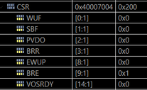
On boot (breakpoint at the top of main) the PWR_CSR register shows the backup regulator is enabled as expected,
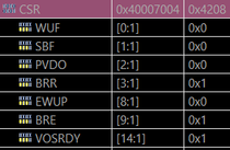
After configuring the backup SRAM, PWR_CSR now shows the backup regulator is ready,
- Mark as New
- Bookmark
- Subscribe
- Mute
- Subscribe to RSS Feed
- Permalink
- Email to a Friend
- Report Inappropriate Content
2023-09-22 2:56 PM
@ONadr.1 - I measure no current into VBAT when VDD is off, but that may just be that the current is too low and in the noise floor of my 1 V/A current monitor. I'll work on setting up a uA-range current measurement.
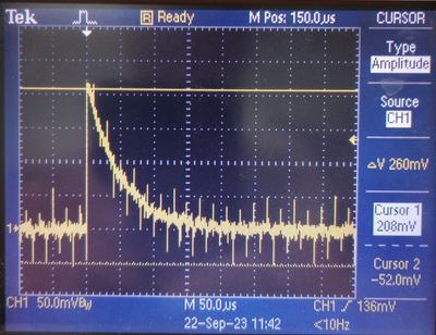
There's a current spike into VBAT when VBAT is off, but connected to a PSU, and VDD is applied (no current spike if not connected to PSU). I don't see any current on VBAT if it's on when VDD is applied. Peak is 260 mV, which equates to 26 mA (1 V/A + 10x turns of wire around probe). I don't know what, if anything, can be inferred from this.
- Mark as New
- Bookmark
- Subscribe
- Mute
- Subscribe to RSS Feed
- Permalink
- Email to a Friend
- Report Inappropriate Content
2023-09-22 3:09 PM - edited 2023-09-22 3:12 PM
Pins 18/19 are VSS/VDD pair, but nonetheless:
[Can't upload image due to Khoros/ST limiting number of images I can upload... Sigh.]
STM32F405/407 datasheet, Power supply schemes chapter: VDDA and VSSA must be connected to VDD and VSS , respectively.
Power supply scheme, footnote: VDDA = VSSA.
Absolute maximum ratings, Variations between different VDD power pins, max. 50mV.
The 0.3V difference in your case is probably not detrimental to actual operation when VDD/VDDA are up, but, the current spike you've described above... have you read the story I've linked to? As reset circuitry which also switches over from VBAT to VDD for the backup-power domain is controlled from VDDA, if VDDA rises later than VDD, the whole mcu is powered from VBAT during that moment.
JW
- Mark as New
- Bookmark
- Subscribe
- Mute
- Subscribe to RSS Feed
- Permalink
- Email to a Friend
- Report Inappropriate Content
2023-09-22 3:35 PM
Correct - pins 18/19 are VSS/VDD, not VSSA/VDDA as shown in the table (dang excel autocomplete).
Funny how often these questions can be answered by reading the datasheet... Thanks for pointing me to the right spot in it! And the link you sent reinforces that this is probably a VDDA != VDD issue.
Section 2.2.14, p. 24 - VDDA and VSSA must be connected to VDD and VSS
Section 5.2, p. 78 - Variations between different VDDx power pins < 50 mV
That looks like my problem. I'm powering VDDA at 3.0V and VDD at 3.3V. I guess I need to make due with filtering 3.3V rather than using a precision 3.0V reference.
Other than the backup SRAM not working right - Are you aware of any other issues with powering VDD and VDDA at different voltages? I have another STM32F405 board that has +3.3V on VDD and +2.5V on VDDA that seems to work fine, though it doesn't use Vbat.
- Mark as New
- Bookmark
- Subscribe
- Mute
- Subscribe to RSS Feed
- Permalink
- Email to a Friend
- Report Inappropriate Content
2023-09-22 3:49 PM
> Are you aware of any other issues with powering VDD and VDDA at different voltages?
No. But I never investigated either, and have no inside information.
I'm not even convinced myself that this is the problem here, even if I might've sounded somewhat confident above, so please let us know of the outcome.
Jan
- STM32H725 internal tamper detection in STM32 MCUs Products
- STM32CubeMX does not preserve conditional RTC initialization (it reinitialize when backup register is set) in STM32CubeMX (MCUs)
- Issues with FM24CLXX_WriteData function in STM32 project in STM32 MCUs Products
- About FAQ: STM32H7 SRAM/Backup SRAM content is not preserved after reset in STM32 MCUs Products


