- STMicroelectronics Community
- STM32 MCUs
- STM32 MCUs Products
- Re: Releasing JTDO/NJTRST from PB3/PB4 for GPIO us...
- Subscribe to RSS Feed
- Mark Topic as New
- Mark Topic as Read
- Float this Topic for Current User
- Bookmark
- Subscribe
- Mute
- Printer Friendly Page
Releasing JTDO/NJTRST from PB3/PB4 for GPIO use
- Mark as New
- Bookmark
- Subscribe
- Mute
- Subscribe to RSS Feed
- Permalink
- Email to a Friend
- Report Inappropriate Content
2016-09-07 5:58 PM
Using a STM32L152RCT6 - currently testing software on 32L152CDISCOVERY board
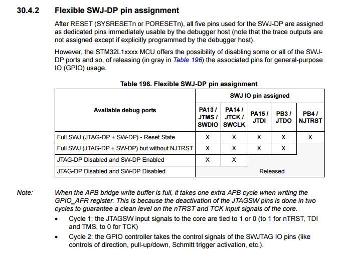
I am trying to configure PB3 (JTDO) as an output GPIO, however I am not able to do so. The pin is always stuck at 1.471V (Vcc/2) Vcc= 2.95.I removed SB101 the solder bridge which connected it to the ST-Link in an attempt to resolve the issue with no luck.PB4 (NJTRST) is having a similar issue, however when a Bit_Reset is written to it by user it resets from ist original state (Pulled up - 2.9V)RM0038 mentions''For user software designs, note that:To release the debug pins, remember that they will first be configured wither in input-pull-up
(nTRST, TMS, TDI) or pull-down (TCK) or output tristate(TDO) for a certain duration after reset
until the instant when the user software releases the pins.
When debug pins (JTAG or SW or TRACE) are mapped, changing the corresponding IO pin
configuration in the IOPORT controller has no effect.''How do I release these pins, PB3 and PB4. Couldn't find any example code or proper explanation. Any suggestions welcome! #!stm32 #stm32l152 #stm32l-jtag-swd-gpio-reuse
- Labels:
-
DEBUG
-
STM32L1 Series
- Mark as New
- Bookmark
- Subscribe
- Mute
- Subscribe to RSS Feed
- Permalink
- Email to a Friend
- Report Inappropriate Content
2016-09-07 11:43 PM
sometimes every you want to know you'll find in the reference-manual of your ST device..
quote:32.4.4 Using serial wire and releasing the unused debug pins as GPIOsTo use the serial wire DP to release some GPIOs, the user software must change the GPIO (PA15, PB3 and PB4) configuration mode in the GPIO_MODER register. This releases PA15, PB3 and PB4 which now become available as GPIOs.- Mark as New
- Bookmark
- Subscribe
- Mute
- Subscribe to RSS Feed
- Permalink
- Email to a Friend
- Report Inappropriate Content
2016-09-08 12:52 AM
Thanks for that chris
GPIO_InitTypeDef GPIO_InitStructure;GPIO_StructInit(&GPIO_InitStructure);GPIO_InitStructure.GPIO_Speed = GPIO_Speed_40MHz;GPIO_InitStructure.GPIO_PuPd = GPIO_PuPd_NOPULL;GPIO_InitStructure.GPIO_Mode = GPIO_Mode_OUT;GPIO_InitStructure.GPIO_Pin = GPIO_Pin_3 | GPIO_Pin_4;GPIO_Init(GPIOB, &GPIO_InitStructure);GPIO_InitStructure.GPIO_Pin = GPIO_Pin_15;GPIO_Init(GPIOA, &GPIO_InitStructure);The above is my code and I believe it does what you quoted. PB3 remains stuck on 1.4V....I am lost as to what I else I can try to solve this.I've already tried remapping an alternate function to the pins... with no luck- Mark as New
- Bookmark
- Subscribe
- Mute
- Subscribe to RSS Feed
- Permalink
- Email to a Friend
- Report Inappropriate Content
2016-09-08 2:57 AM
1. you have to change your debug-settings from JTAG to SWD. if you change mode pins will debugging with JTAG your debug-session is likely to crash.
2. change to the desired mode, e.g. output-pushpull with HAL_GPIO_Init()3. set the pin when in output to desired level, e.g. HAL_GPIO_WritePin( , GPIO_PIN_RESET)4. check your hardware / schematic if you have some connected components on this pin/net which mess up your voltage-level- Mark as New
- Bookmark
- Subscribe
- Mute
- Subscribe to RSS Feed
- Permalink
- Email to a Friend
- Report Inappropriate Content
2016-09-11 4:18 PM
I've done all the steps and the problem is still persistent...
Here's a video of what happens https://www.youtube.com/watch?v=RZcpJspHfP8- Mark as New
- Bookmark
- Subscribe
- Mute
- Subscribe to RSS Feed
- Permalink
- Email to a Friend
- Report Inappropriate Content
2016-09-11 5:54 PM
Remove the LCD/GLASS
Up vote any posts that you find helpful, it shows what's working..
- Mark as New
- Bookmark
- Subscribe
- Mute
- Subscribe to RSS Feed
- Permalink
- Email to a Friend
- Report Inappropriate Content
2016-09-11 8:45 PM

- Mark as New
- Bookmark
- Subscribe
- Mute
- Subscribe to RSS Feed
- Permalink
- Email to a Friend
- Report Inappropriate Content
2016-09-12 2:12 AM
This is how CubeMx does it:
First make the pins low, then setup for output.static void MX_GPIO_Init(void)
{
GPIO_InitTypeDef GPIO_InitStruct;
/* GPIO Ports Clock Enable */
__HAL_RCC_GPIOB_CLK_ENABLE();
__HAL_RCC_GPIOA_CLK_ENABLE();
/*Configure GPIO pin Output Level */
HAL_GPIO_WritePin(GPIOB, GPIO_PIN_4|GPIO_PIN_3, GPIO_PIN_RESET);
/*Configure GPIO pins : PB4 PB3 */
GPIO_InitStruct.Pin = GPIO_PIN_4|GPIO_PIN_3;
GPIO_InitStruct.Mode = GPIO_MODE_OUTPUT_PP;
GPIO_InitStruct.Pull = GPIO_NOPULL;
GPIO_InitStruct.Speed = GPIO_SPEED_FREQ_LOW;
HAL_GPIO_Init(GPIOB, &GPIO_InitStruct);
}- Stm32f411ce firmware write failing. in STM32 MCUs Products
- STM32H5 MCU Package Update Changes Peripheral Pinouts (No Release Notes Found) in STM32CubeMX (MCUs)
- Linking errors of examples with new STM32WBA release 1.6 & Cannot launch debugger in VS Code in STM32 MCUs Wireless
- STM32CubeProgrammer v2.19 released in STM32CubeProgrammer (MCUs)
- STM32CubeIDE 1.18.0 released in STM32CubeIDE (MCUs)