- STMicroelectronics Community
- STM32 MCUs
- STM32 MCUs Products
- Fluctuations in ADC value of STM32H743 MCU
- Subscribe to RSS Feed
- Mark Topic as New
- Mark Topic as Read
- Float this Topic for Current User
- Bookmark
- Subscribe
- Mute
- Printer Friendly Page
Fluctuations in ADC value of STM32H743 MCU
- Mark as New
- Bookmark
- Subscribe
- Mute
- Subscribe to RSS Feed
- Permalink
- Email to a Friend
- Report Inappropriate Content
2018-10-23 11:41 AM
Hi,
I have been working with STM ADC’s from quite a long time. I had used STM32F373 and F4 series MCU ADC’s earlier for my applications. As, now my application requires huge amount of RAM, memory and computation speed I have shifted to STM32H743 MCU . Earlier when I used F3 series ADC the noisy LSB was around 4 LSB which is a quite good resolution for 16 bit ADC . But as I have shifted to STM32H743 the noise level fluctuation is around 300LSB for 16 bit ADC resolution for single ended channel. When I hook up ground to ADC pin it shows a value fluctuation of about 100LSB . I use Analog accelerometer for my application and I need to see a resolution of 1 mg and with such amount of noise I won’t be able to achieve such high resolution.
The code is generated using CubeMx.The ADC is clocked using external clock and the MCU is powered from a 3.3 V regulator supply and Analog and digital grounds are properly separated.
I checked into their errata sheet and I couldn’t find any possible solution.
Any solutions will be highly appreciated .
Thank you
Solved! Go to Solution.
- Labels:
-
ADC
-
STM32H7 series
- Mark as New
- Bookmark
- Subscribe
- Mute
- Subscribe to RSS Feed
- Permalink
- Email to a Friend
- Report Inappropriate Content
2019-09-13 4:26 AM
We had also some issues to avoid ADC "glitches" up to 2000 digits at 16 Bit mode...
Disabling the DAC solve this problem (disable the DAC buffer reduce the problem). The DAC brings strange voltage spikes to VRef+.... I don't know why, because the driving voltage should be AVCC not VRef+.
- Mark as New
- Bookmark
- Subscribe
- Mute
- Subscribe to RSS Feed
- Permalink
- Email to a Friend
- Report Inappropriate Content
2019-09-13 9:44 AM
Wonderful analysis! I don't have experience with the STM32H743 yet but consider adding the following to your next steps:
1) Stop the processor during the ADC conversion - do a WFI() and see if that helps. If this helps, then, it is on chip or board noise coupling.
2) What is the source impedance of the channel? I would try adding an Op-Amp (temporarily) to see if that helps
3) Another thing to try is to do these measurements while sweeping the sampling time from min to max. If this affects things, then, it points to a source impedance / STM32H7 ADC input circuit interaction.
- Mark as New
- Bookmark
- Subscribe
- Mute
- Subscribe to RSS Feed
- Permalink
- Email to a Friend
- Report Inappropriate Content
2019-09-13 10:12 AM
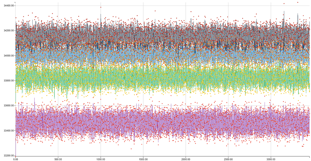
Here 2x ADC modules with 2 channles per each during simultaneous sampling each pair of channels at much lower frequecy (~13 kSPS)
Basically - the range of min-max values are are the same, as at the high frequency. But you can't not see that there is some aliasing happening because sampling speed is slower by a factor of hundreds. So the noise looks completely random.
I do have a unity-gain buffer on each channel between my sensor circuitry and ADC inputs of STM32H7. In fact for the purity of tests I've connected the ADC input to a AA battery. Also if trying to measure DC level (like a battery voltage) - the source impedance might not need to be very low, since sample and hold capacitor stays charged at the same level between samples.
I've came to understanding that the ripple I see on AVdd is exactly double of sampling frequency. Because I actually have 2 channels enabled per ADC module in scan mode. The sampling is triggered by timer that runs twice faster than the needed sampling frequency per single channel. So the observed ripple appears to be the sag of supply voltage when ADC preforms sample conversion on each channel. So there is no guarantee it restores to exactly the same level before S/H on the next channel, and that is actually expected to produce such aliasing-like strange effects (assuming if the level of AVdd sag is dependent on the actual converted value).
I still have to run the testing with proper dedicated AVdd supply. The ferrite bead installed on Nucleo boar may represent high AVdd supply impedance when sampling frequency is very high. Also if it sags during conversion itself - than the Vref is changing as well while converting each subsequent bit.
Accordingly the actual ADC clock may play a major role here as well. Clocking ADC slower should make AVdd sag during conversion less steep or non existent at all (just some spikes on each bit conversion). What I am trying to say is that changing the clock of sampling timer (that triggers my ADC module) probably did not help because ADC was still running at a very high clock rate. I had to reduce the ADC clock frequency to the minimum as well, so the expectation will be less diturbance on AVdd and more pure conversion result.
All these "reduce speed" tricks however won't work for my application because I need high sampling speeds (at least 2MSPS per channel for 4 channels).
- Mark as New
- Bookmark
- Subscribe
- Mute
- Subscribe to RSS Feed
- Permalink
- Email to a Friend
- Report Inappropriate Content
2019-09-25 11:15 AM
Any updates / progress on reducing the noise on the STM32H743 ADC?
- Mark as New
- Bookmark
- Subscribe
- Mute
- Subscribe to RSS Feed
- Permalink
- Email to a Friend
- Report Inappropriate Content
2019-10-10 10:38 PM
PROBLEM SOLVED
Appears to be an issue of the Nucleo-144 demo-board itself (NUCLEO-H743ZI specifically), NOT AN STM32H7 FAULT!
HOW TO FIX?
- Desolder/remove L2 ferrite bead to disable Ethernet PHY chip (see Nucleo-144 schematic, it is located close to that IC nearby Ethernet port).
- Or use NUCLEO board without Ethernet hardware (OOOPS ... not available for H7)
- Alternatively you may remove SB2, but that will disable USB-port circuitry as well
WHY?
- This chip designated to PAM-modulate and amplify the Ethernet signal before feeding it into long wires of CAT5/6 cable.
- Apparently it does not have any low-power/standby mode when not in use.
- So even if you not use it - its clock (25MHz) injected into board circuitry (my guess - over the ground). Observed at ADC with 5mV peak-to-peak swing, basically reducing ADC resolution to 10-bits!
Can you have Ethernet and clean ADC capture at the same time?
- Somewhat possible with oversampling or moving-average filter.
- 16-samples needed to get 12 effective bits of resolution, but limits your acquisition bandwidth to around 100kHz
And here is my story of how did I figured it out:
First of all - sorry for a delay since my last reply. To approach this problem I had to wait for a good weekend (free of other tasks and events) since I decided to go "full ballistic" to eliminate any guess work:
- The Nucleo-144 board has been put into 3D-printed enclosure which was painted with MG Chemicals Super Shield conductive paint to block any external EMI sources.
- I've wired ADC inputs to 1.5V AAA battery. The wires were as short as I could get and battery did fit into shielded enclosure of the Nucleo board.
- I've used external power supply 8..12V.
- Also the ADC analog block (AVDD) was powered form the same LDO as the MCU itself. So MCU digital blocks can interfere with the ADC. It is always recommeded to use separate supply and even dedicated Vref for ADC. So I've soldered a separate circuit with 3.3V LDO isolated from the main external supply by capacitance multiplier (see EEVBolg youtube video on what is that: https://youtu.be/wopmEyZKnYo ).
- So SB12 (see Nucleo schematic) was de-soldered to connect this new clean-output LDO to AVDD. SBL162 was de-soldered as well and AGND was wired directly to the LDO ground pin. In other words AVDD and AGND of the nucleo board were now wired directly to its dedicated LDO.
- Test DC-signal source , the negative tab of 1.5V AAA battery was wired to the LDO ground. Eliminating ground loops for signal source.
- Add more bypass-capacitors for analog supply pins (soldered few more MLCCs on top of C34)
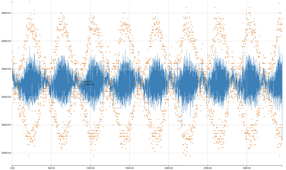
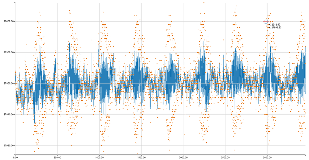
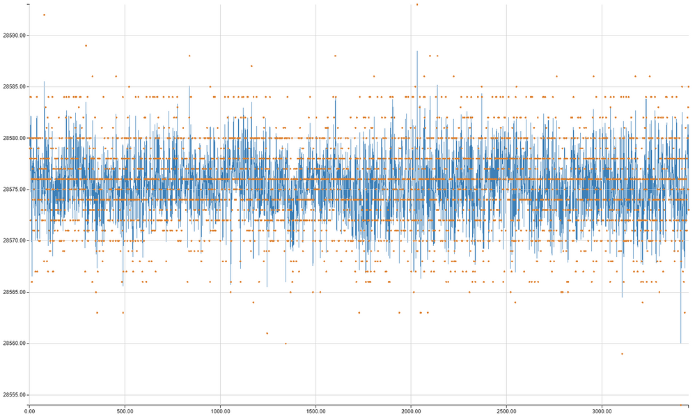
And then I've got the same high-speed (2 MSPS) raw data captures again:
as you see it still shows this aliasing affect, but it looks now way cleaner and more "pronounced" than it was before:
If using moving average filter using 2 samples, it improves slightly:
Trying to run ADC at its maximum sampling speed (5MSPS) did not help to figure out interference frequency, so it is higher than that.
As I've already mentioned in my previous post - you can not identify that this is aliasing of higher-frequency interference IF you do slow sampling. As in this 13kSPS example it just looks like Gaussian noise, because clock drift (PLL jitter) introduces a lot of phase noise to notice any aliasing patterns of 13kHz vs 25MHz interference.
For these who don't now:
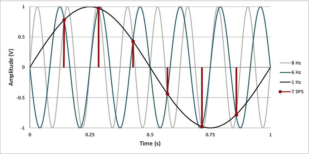
ADC aliasing happens when there is higher frequency at your ADC input than the Nyquist frequency (more than 1/2 of you sampling speed). You can not work with this kind of acquired data if you want to do any decent signal processing on it. In all good designs ADC inputs are guarded with good low-pass filters. Here is good example from the web (https://e2e.ti.com/blogs_/archives/b/precisionhub/archive/2015/09/04/aliasing-in-adcs-not-all-signals-are-what-they-appear-to-be)
As you see 6 and 8 Hz signals can not be reproduced properly when sampling at 7Hz, you see that as 1Hz signal on ADC output.
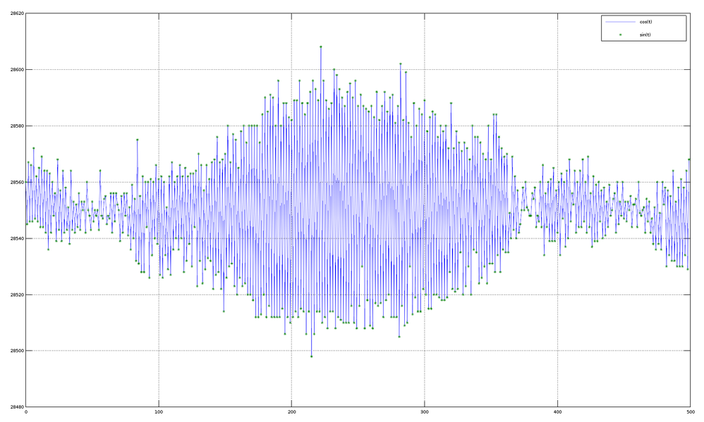
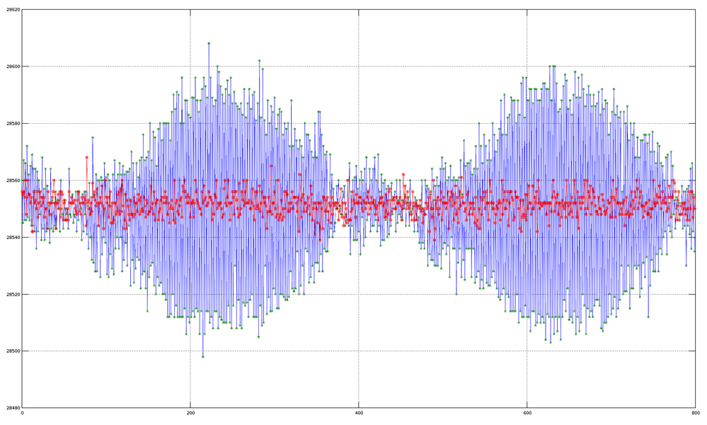
In our case - the parasitic input was way beyond my Nyquist frequency of 1Mhz. If we zoom-in time scale of the first picture and plot it in MATLAB:
The parasitic signal is apparently at 5mV peak to peak range (100 LSB out of 65536 for 3.3V full range).
Since all external sources were eliminated by shielding and ADC is powered by dedicated clean LDO there are few reasons left:
- Internal issue in STM32H7 - highly unlikely. In datasheet we have SINAID specified at 82dB for single-ended input. If my calculations are correct - it should be equivalent of 5LSB RMS-noise. In other words - if measuring a perfect DC signal (from AAA-battery) 68% of samples should be with-in 10LSB range, and 99.7% for Gaussian noise should be with-in 30LSB peak-to-peak range.
- Interfering signal source is some other component on the Nucleo-144 board, could be ST-Link as well getting something from USB-grouding.
To figure this out you need a spectrum analyser, LNA amplifier and H-field probe (https://youtu.be/crs_QLuUTyQ)
You can go cheaper way and get an SDR radio USB dongle with self-made H-field probe (https://www.stupid-projects.com/emc-probe-using-rtl-sdr)
I've found and ordered an MSi.SDR that has a perfect range for 10kHz to 2GHz for MCU board purposes.
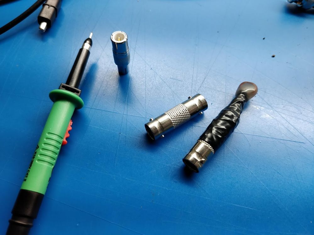
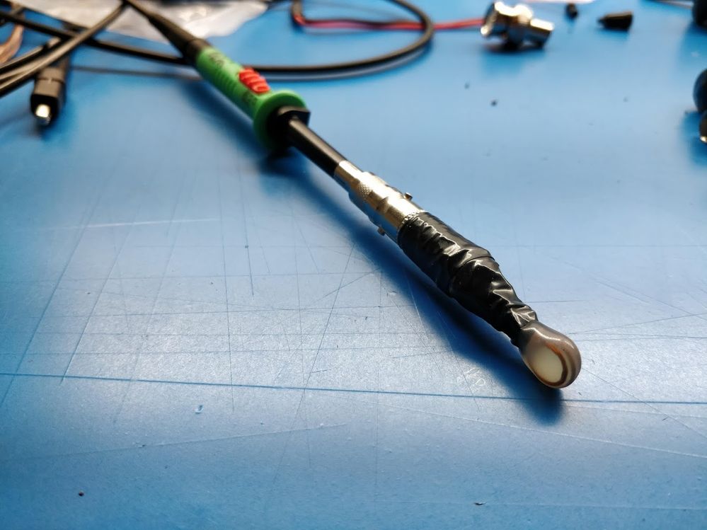
Without having a patience to wait for SDR and semi-rigid coax delivery I've used an oscilloscope probe which came tip-to-BNC adapter. Using another female-to-feamale BNC-connector, piece of copper wire, aluminum foil and electric tape I've got an E/H-probe in like 20 min:
With this contraption I was simply observing waveform on the scope and sniffed the interference source when I've stick it into Ethernet PHY IC package. I was lucky it was powerful enough to get me 5mV spikes on the scope without the need of any LNA.
Here is the raw sampling after I've thrown away an L2 ferrite bead. It should actually serve as a filter connecting a +3V3V_PER peripherals supply line to Ethernet PHY circuitry, but apparently interference is so strong that it propagates through the ground, or EMI into the wires connecting my DC-signal source to ADC input(s).
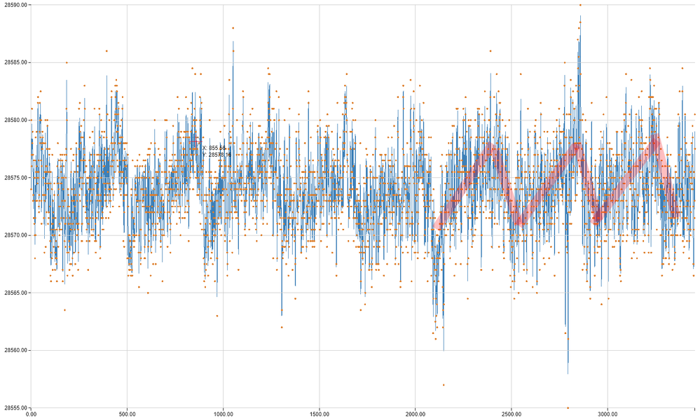
Here is the RAW capture of DC-signal source (AAA battery) after the hack:
And here its overlay (red) with the RAW capture before disabling Ethernet PHY (blue):
As you see - I've got it all well within spec, major half of samples are somewhat in 10LSB peak to peak range, while all of them within 30LSB.
- Mark as New
- Bookmark
- Subscribe
- Mute
- Subscribe to RSS Feed
- Permalink
- Email to a Friend
- Report Inappropriate Content
2019-10-12 8:04 PM
Got my MSi.SDR delivered, so made an H-field probe to see more what spectrum is radiated from Ethernet PHY chip:
Using RSP Spectrum Analyser software, here is the spectrum when the probe is far away from the Ethernet PHY chip:
And this is when the probe is close as shown on the picture above:

- Mark as New
- Bookmark
- Subscribe
- Mute
- Subscribe to RSS Feed
- Permalink
- Email to a Friend
- Report Inappropriate Content
2019-10-14 2:03 AM
Thanks a lot for this great analysis.
I can confirm that removing the ferrite bead of the PHY drastically improves the analog performance.
I tested it with a NUCLEO-H743ZI2 eval board and also with custom board which uses a different PHY.
- Mark as New
- Bookmark
- Subscribe
- Mute
- Subscribe to RSS Feed
- Permalink
- Email to a Friend
- Report Inappropriate Content
2019-10-22 12:01 PM
Hey Matthias,
I have unrelated question:
You've mentioned that you use newer NUCLEO H743ZI2 (I've am using a regular ZI).
Does your board has newer revision "V" of STM32H7 on it? The one that can run at 480MHz?
- Mark as New
- Bookmark
- Subscribe
- Mute
- Subscribe to RSS Feed
- Permalink
- Email to a Friend
- Report Inappropriate Content
2019-10-22 12:13 PM
Unrelated update:
So SDR appears to be a great cheap alternative replacement for Spectrum Analyzer to do near-field E/H-emissions testing. Or troubleshooting interference sources as it was discovered with Nucleo STM32H7 board in this thread.
After some more researching in SDR comunity I've figured that MSi.SDR while beeing the cheapest radio capable to pickup in kHz band - is not the ideal.
MSi.SDR is a cheap Chinese clone of RSP1 from SDRPlay. It has issues with spectrum output when there are no signal connected (no antennae or probe on its input) - see my first picture of the spectrum in previous post. It has spurs of 24Mhz and some of its multiples (48MHz, 120Mhz, 144Mhz).
24MHz - is the XTAL you may find on MSi.SDR board if you take it apart.
Today for around $100 you can get RSP1A (an updated version of RSP1). It has stellar sensitivity (like 20..30dB lower than MSi.SDR) and as per what i see on youtube reviews - with no spurs.
- Mark as New
- Bookmark
- Subscribe
- Mute
- Subscribe to RSS Feed
- Permalink
- Email to a Friend
- Report Inappropriate Content
2019-10-22 10:20 PM
Yes, my NUCLEO H743ZI2 has a Revision V Chip on it.
- USB OTG HS Host: PENA cleared spuriously at HFNUM=16383 with ULPI PHY (USB3300) in STM32 MCUs Embedded software
- TouchGFX Application Shows Black Screen After Bootloader Jump in STM32 MCUs TouchGFX and GUI
- STM32H753 Ethernet TX corruption in STM32 MCUs Embedded software
- STM32H743 - Setting External Event source for HRTIM Timer in CubeMX ? in STM32CubeMX (MCUs)
- No STM32 target found in STM32CubeProgrammer (MCUs)

