- STMicroelectronics Community
- STM32 MCUs
- STM32 MCUs Products
- Fluctuations in ADC value of STM32H743 MCU
- Subscribe to RSS Feed
- Mark Topic as New
- Mark Topic as Read
- Float this Topic for Current User
- Bookmark
- Subscribe
- Mute
- Printer Friendly Page
Fluctuations in ADC value of STM32H743 MCU
- Mark as New
- Bookmark
- Subscribe
- Mute
- Subscribe to RSS Feed
- Permalink
- Email to a Friend
- Report Inappropriate Content
2018-10-23 11:41 AM
Hi,
I have been working with STM ADC’s from quite a long time. I had used STM32F373 and F4 series MCU ADC’s earlier for my applications. As, now my application requires huge amount of RAM, memory and computation speed I have shifted to STM32H743 MCU . Earlier when I used F3 series ADC the noisy LSB was around 4 LSB which is a quite good resolution for 16 bit ADC . But as I have shifted to STM32H743 the noise level fluctuation is around 300LSB for 16 bit ADC resolution for single ended channel. When I hook up ground to ADC pin it shows a value fluctuation of about 100LSB . I use Analog accelerometer for my application and I need to see a resolution of 1 mg and with such amount of noise I won’t be able to achieve such high resolution.
The code is generated using CubeMx.The ADC is clocked using external clock and the MCU is powered from a 3.3 V regulator supply and Analog and digital grounds are properly separated.
I checked into their errata sheet and I couldn’t find any possible solution.
Any solutions will be highly appreciated .
Thank you
Solved! Go to Solution.
- Labels:
-
ADC
-
STM32H7 Series
Accepted Solutions
- Mark as New
- Bookmark
- Subscribe
- Mute
- Subscribe to RSS Feed
- Permalink
- Email to a Friend
- Report Inappropriate Content
2019-10-10 10:38 PM
PROBLEM SOLVED
Appears to be an issue of the Nucleo-144 demo-board itself (NUCLEO-H743ZI specifically), NOT AN STM32H7 FAULT!
HOW TO FIX?
- Desolder/remove L2 ferrite bead to disable Ethernet PHY chip (see Nucleo-144 schematic, it is located close to that IC nearby Ethernet port).
- Or use NUCLEO board without Ethernet hardware (OOOPS ... not available for H7)
- Alternatively you may remove SB2, but that will disable USB-port circuitry as well
WHY?
- This chip designated to PAM-modulate and amplify the Ethernet signal before feeding it into long wires of CAT5/6 cable.
- Apparently it does not have any low-power/standby mode when not in use.
- So even if you not use it - its clock (25MHz) injected into board circuitry (my guess - over the ground). Observed at ADC with 5mV peak-to-peak swing, basically reducing ADC resolution to 10-bits!
Can you have Ethernet and clean ADC capture at the same time?
- Somewhat possible with oversampling or moving-average filter.
- 16-samples needed to get 12 effective bits of resolution, but limits your acquisition bandwidth to around 100kHz
And here is my story of how did I figured it out:
First of all - sorry for a delay since my last reply. To approach this problem I had to wait for a good weekend (free of other tasks and events) since I decided to go "full ballistic" to eliminate any guess work:
- The Nucleo-144 board has been put into 3D-printed enclosure which was painted with MG Chemicals Super Shield conductive paint to block any external EMI sources.
- I've wired ADC inputs to 1.5V AAA battery. The wires were as short as I could get and battery did fit into shielded enclosure of the Nucleo board.
- I've used external power supply 8..12V.
- Also the ADC analog block (AVDD) was powered form the same LDO as the MCU itself. So MCU digital blocks can interfere with the ADC. It is always recommeded to use separate supply and even dedicated Vref for ADC. So I've soldered a separate circuit with 3.3V LDO isolated from the main external supply by capacitance multiplier (see EEVBolg youtube video on what is that: https://youtu.be/wopmEyZKnYo ).
- So SB12 (see Nucleo schematic) was de-soldered to connect this new clean-output LDO to AVDD. SBL162 was de-soldered as well and AGND was wired directly to the LDO ground pin. In other words AVDD and AGND of the nucleo board were now wired directly to its dedicated LDO.
- Test DC-signal source , the negative tab of 1.5V AAA battery was wired to the LDO ground. Eliminating ground loops for signal source.
- Add more bypass-capacitors for analog supply pins (soldered few more MLCCs on top of C34)
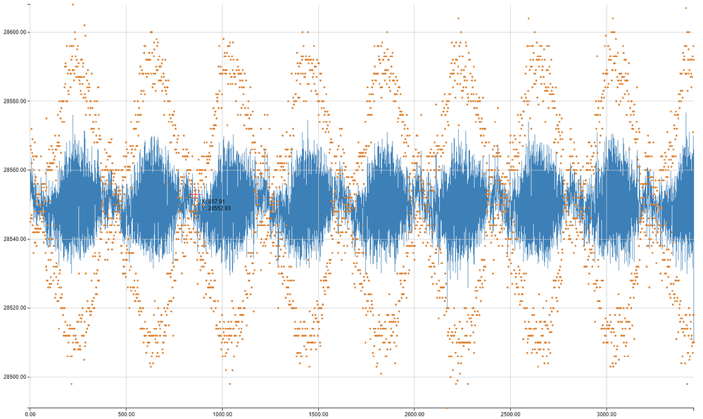
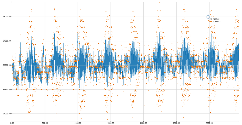
And then I've got the same high-speed (2 MSPS) raw data captures again:
as you see it still shows this aliasing affect, but it looks now way cleaner and more "pronounced" than it was before:
If using moving average filter using 2 samples, it improves slightly:
Trying to run ADC at its maximum sampling speed (5MSPS) did not help to figure out interference frequency, so it is higher than that.
As I've already mentioned in my previous post - you can not identify that this is aliasing of higher-frequency interference IF you do slow sampling. As in this 13kSPS example it just looks like Gaussian noise, because clock drift (PLL jitter) introduces a lot of phase noise to notice any aliasing patterns of 13kHz vs 25MHz interference.
For these who don't now:
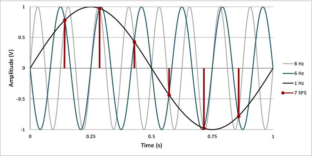
ADC aliasing happens when there is higher frequency at your ADC input than the Nyquist frequency (more than 1/2 of you sampling speed). You can not work with this kind of acquired data if you want to do any decent signal processing on it. In all good designs ADC inputs are guarded with good low-pass filters. Here is good example from the web (https://e2e.ti.com/blogs_/archives/b/precisionhub/archive/2015/09/04/aliasing-in-adcs-not-all-signals-are-what-they-appear-to-be)
As you see 6 and 8 Hz signals can not be reproduced properly when sampling at 7Hz, you see that as 1Hz signal on ADC output.
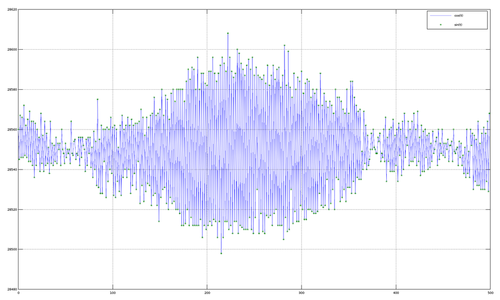
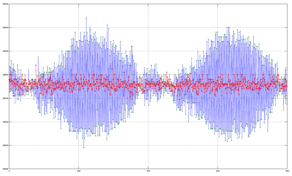
In our case - the parasitic input was way beyond my Nyquist frequency of 1Mhz. If we zoom-in time scale of the first picture and plot it in MATLAB:
The parasitic signal is apparently at 5mV peak to peak range (100 LSB out of 65536 for 3.3V full range).
Since all external sources were eliminated by shielding and ADC is powered by dedicated clean LDO there are few reasons left:
- Internal issue in STM32H7 - highly unlikely. In datasheet we have SINAID specified at 82dB for single-ended input. If my calculations are correct - it should be equivalent of 5LSB RMS-noise. In other words - if measuring a perfect DC signal (from AAA-battery) 68% of samples should be with-in 10LSB range, and 99.7% for Gaussian noise should be with-in 30LSB peak-to-peak range.
- Interfering signal source is some other component on the Nucleo-144 board, could be ST-Link as well getting something from USB-grouding.
To figure this out you need a spectrum analyser, LNA amplifier and H-field probe (https://youtu.be/crs_QLuUTyQ)
You can go cheaper way and get an SDR radio USB dongle with self-made H-field probe (https://www.stupid-projects.com/emc-probe-using-rtl-sdr)
I've found and ordered an MSi.SDR that has a perfect range for 10kHz to 2GHz for MCU board purposes.
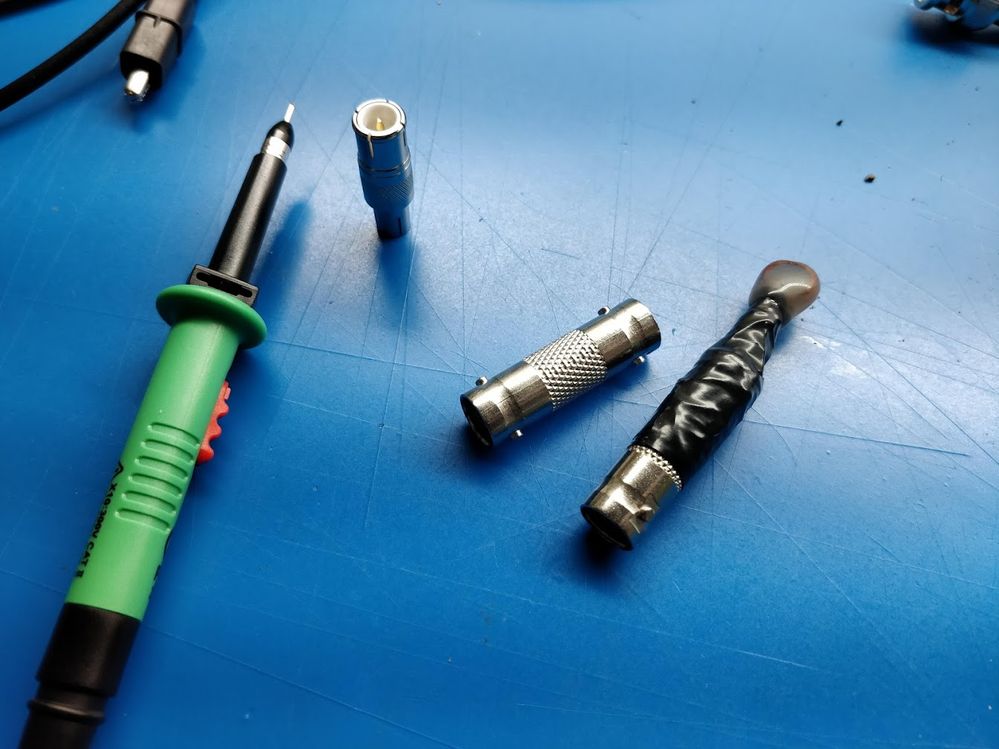
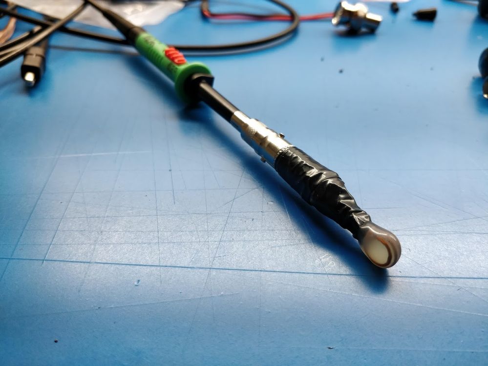
Without having a patience to wait for SDR and semi-rigid coax delivery I've used an oscilloscope probe which came tip-to-BNC adapter. Using another female-to-feamale BNC-connector, piece of copper wire, aluminum foil and electric tape I've got an E/H-probe in like 20 min:
With this contraption I was simply observing waveform on the scope and sniffed the interference source when I've stick it into Ethernet PHY IC package. I was lucky it was powerful enough to get me 5mV spikes on the scope without the need of any LNA.
Here is the raw sampling after I've thrown away an L2 ferrite bead. It should actually serve as a filter connecting a +3V3V_PER peripherals supply line to Ethernet PHY circuitry, but apparently interference is so strong that it propagates through the ground, or EMI into the wires connecting my DC-signal source to ADC input(s).
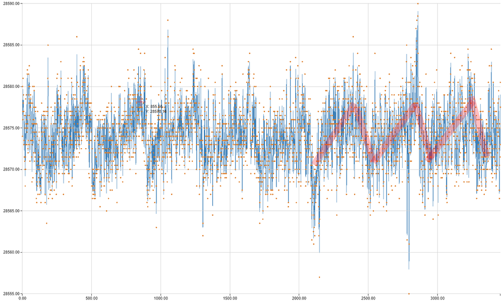
Here is the RAW capture of DC-signal source (AAA battery) after the hack:
And here its overlay (red) with the RAW capture before disabling Ethernet PHY (blue):
As you see - I've got it all well within spec, major half of samples are somewhat in 10LSB peak to peak range, while all of them within 30LSB.
- Mark as New
- Bookmark
- Subscribe
- Mute
- Subscribe to RSS Feed
- Permalink
- Email to a Friend
- Report Inappropriate Content
2018-10-24 03:27 AM
Hi @James ,
With the STM32F373 MCU, you were using an 12-bit ADC. Now with the STM32H743, you have a 16-bit one. Thus, it's normal that the noise level is more important using the STM32H7.
However, 100 LSB when the ADC is grounded stills a high value.
Are you performing a SW ADC calibration? This is mandatory in in order to improve the conversion accuracy. If you're using ST drivers, this is done through function "HAL_ADCEx_Calibration_Start".
PS: You have highlighted that you have read the STM32H7 errata-sheet, please make sure that you're not facing one of the ADC limitations described there.
Khouloud
- Mark as New
- Bookmark
- Subscribe
- Mute
- Subscribe to RSS Feed
- Permalink
- Email to a Friend
- Report Inappropriate Content
2018-10-24 03:54 AM
> The ADC is clocked using external clock and the MCU is powered from a 3.3 V regulator supply and Analog and digital grounds are properly separated.
Have you checked the stability of VDDA ?
I would be wary of the high speed (= high power) characteristics of the H7, and consider an external ADC. Or an accelerometer with digital interface.
- Mark as New
- Bookmark
- Subscribe
- Mute
- Subscribe to RSS Feed
- Permalink
- Email to a Friend
- Report Inappropriate Content
2018-10-25 12:15 PM
Hi Khouloud,
Thank you very much for your reply. In STM32F373 MCU I was using 16 bit SDADC (Sigma Delta) and even for 16 bit ADC the noise was around 4 LSB.
But now when I compare the results of 12bit and 16bit ADC of STM32H743 it seems that there is just 4 bit amplification in the results.
I am using HAL libraries and even after doing calibration the results are similar no change. Now I seriously stuck with this noise problem.
James
- Mark as New
- Bookmark
- Subscribe
- Mute
- Subscribe to RSS Feed
- Permalink
- Email to a Friend
- Report Inappropriate Content
2018-10-25 12:21 PM
Hi AVa Tar,
Thank you very much for your reply. I checked the stability of the power supply it is quite stable and even I have bypass capacitor banks on PCB and it’s a 4 layer PCB so the power supply should be good.
My application needs around 10K bandwidth and I couldn’t find any digital accelerometers with such high bandwidth so decided to use Analog accelerometer.
Ranjith
- Mark as New
- Bookmark
- Subscribe
- Mute
- Subscribe to RSS Feed
- Permalink
- Email to a Friend
- Report Inappropriate Content
2018-10-25 01:36 PM
good project, I guess that you have a noise problem.. It is a custom board ?
they are quite specific about the 2.2uF Low ESR caps, did you use those ?
do you have SDRAM on your board ? ( very noisy)
can you supply the board from a battery not a switcher ?
Then you may see an improvement.
I would add more power supply filtering and ADC power filtering.
What impedance is the input drive ?
maybe you need to buffer the signal with an opamp
Edit:
Where did you join the Analog ground to the Digital ground ?
- Mark as New
- Bookmark
- Subscribe
- Mute
- Subscribe to RSS Feed
- Permalink
- Email to a Friend
- Report Inappropriate Content
2018-11-02 08:31 AM
Hi @James
I advise you to have a look on the following recommendations and check if they are satisfied in your HW:
1) ADC voltage reference: Need low offset, low drift, and low-noise reference voltage.
2) Decoupling capacitors :
• A pair of decoupling capacitor on Vref+ and on VDDA (1µFand 10nF) low inductive (0402 package recommended) ; should be placed very close to the MCU (especially the 10nF).
• Each power supply pair should be decoupled with filtering ceramic capacitors (100 nF) and one single tantalum or ceramic capacitor (min. 4.7 μF) connected in parallel. These capacitors need to be placed as close as possible to, or below, the appropriate pins on the underside of the PCB.
3) PCB recommendation:
• Solid ground plane and PCB partitioned into analog and digital sections to prevent digital noise from interfering with analog sensitive signals.
4) ADC input Filter :
• 1 Capacitor to GND (47 pF recommended but value depends on application) to be placed very close to ADC input (will act as charge reservoir for current spikes when sampling switch is closed)
• One resistor in series (value depends on application) in case filtering is needed.
Khouloud.
- Mark as New
- Bookmark
- Subscribe
- Mute
- Subscribe to RSS Feed
- Permalink
- Email to a Friend
- Report Inappropriate Content
2019-01-21 10:06 AM
I don't know your setup, but quite a few limitation items exist on the STM32H743 errata sheet from ST: https://www.st.com/content/ccc/resource/technical/document/errata_sheet/group0/b8/f4/b7/a3/d1/a0/44/a6/DM00368411/files/DM00368411.pdf/jcr:content/translations/en.DM00368411.pdf
You might check the work-arounds listed. (This assumes you're using Revision Y silicon.)
- Mark as New
- Bookmark
- Subscribe
- Mute
- Subscribe to RSS Feed
- Permalink
- Email to a Friend
- Report Inappropriate Content
2019-06-07 02:51 AM
Hi @James
did you find a solution for the noise problem?
I have the same problem with the 16 bit ADC of the STM32H7: 300 - 350 LSBs of noise on my signal.
I also used the ADCs of the STM32F3 and F4 in the past an had no issues there.
With the STM32H7 I see the noise on my custom board and also on the NUCLEO-H743ZI Board.
On the nucleo board I tied a 22k/10k voltage divider from 3V3 to PA6 and measured it with ADC1. I also added 100 nF for filtering.
The values which I get from the ADC vary between 20333 and 20682.
Matthias
- Mark as New
- Bookmark
- Subscribe
- Mute
- Subscribe to RSS Feed
- Permalink
- Email to a Friend
- Report Inappropriate Content
2019-08-22 04:07 PM
Last few weeks I've been evaluating Nucleo-144 board with STM32H743ZI. Experiencing similar issue I would like to share my findings here.
According to spec for single-ended Rev Y (400Mhz) the given EOB/SNR/SINAID in ideal scenario we should result int noise fluctuations of around 16LSB (maybe higher occasional peak-to-peak values, but majority of samples should stay in this range), not 200..300 as reported.
So far I think Nucleo-144 H743ZI board does not have sufficient decoupling for AVDD and Vref pins, high-frequency noise is injected into conversion which produces aliasing errors, making some DSP post-processing in my application quite inaccurate. The ADC itself, when turns ON creates fluctuations on AVDD line, that loops back over Vref.
So, I am sampling 4 channels with 2 ADCs, where each ADC scans through two assigned channels (2.6 MHz, so 1.3MHz sampling rate per channel).
I am have configured DMA with double-buffering to eventually run DSP processing in background, without the need to ever stop ADC acquisition.
On the oscilloscope images:
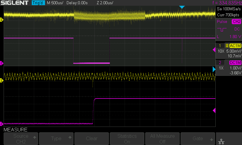
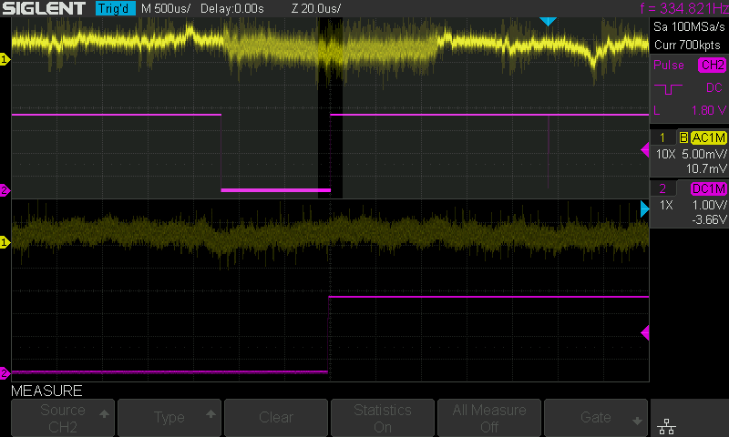
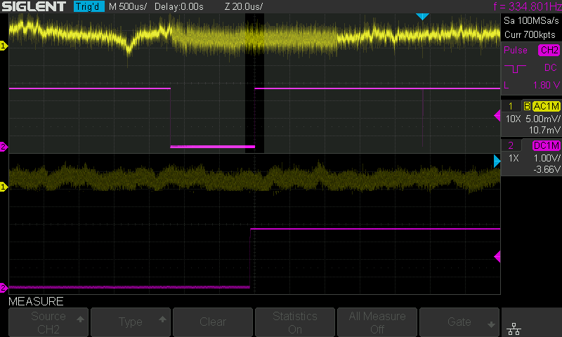
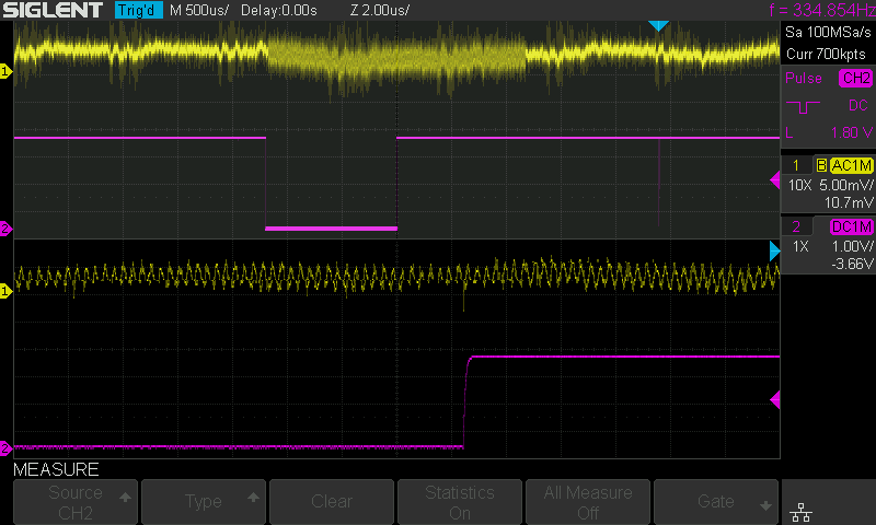
- Yellow channel is AVDD (AC-coupled) where scope probe is hooked to AVDD and AGND pinheaders of the Nucleo 144.
- Pink channel is an onboard blue LED, which goes down when ADC acquisition starts and goes up when DMA half-transfer complete. So main thread begins processing of first half-buffer, while second half-buffer acquisition still in progress. Half buffer length 1728 samples (full buffer is 3456). Since ADC multiplaxes between two channels - there are total 6912 samples acquired.
So to troubleshoot the problem first thing is to figure out and mitigate all the contributing noise sources.
External battery supply with NO USB connected,:
Here how noisier it becomes with connected USB ground:
And here is the same (with battery power and connected USB) with added electrolytic capacitor on AVDD and AGND pin.
A miserable attempt to improve analog supply decoupling, looks slightly cleaner. But with grain of salt - cap inserted on the line between MCU pins and scope input, so it could be just "LPF-ing" the signal which goes into oscilloscope probe, while the analog supply itself is still noisy:
Here is AVDD line with slighly better zoom in time domain:
Attention - my scope is 100MHz bandwidth, so what you see might be aliasing of much higher frequencies.
Anyway 5 mV p-p fluctuation is likely contributes to sampled values accordingly.
With 3.3V supply on Vref a 5mV noise will result into 2.5mV error of measured signal that is half of sumplu line (1.6V) and that is eqvivalent of ~100LSB. Moreover - for a signal that is closer to 3.3V supply line it will increase to 200LSB.
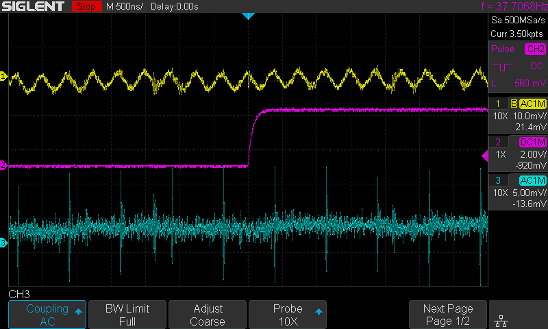
On next scope screenshot the new blue channel is hooked up to one of the ADC channels (pin-header of the Nucleo board). For an experiment I've disconnected the analog circuitry of my sensor and dropped in a pre-charged capacitor. So I get a steady fixed DC input into ADC:
These spikes on the channel line are actual moments when ADC performs "sampling" phase in its "sample and hold" circuitry (latching to charge an internal capacitor).
This seem to be in-sync with fluctuations on AVDD line (yellow). But you see that AVDD level fluctuation is double the frequency than spikes on the ADC channel line - that is because I have an ADC module configured to multiplex between two input channels. So AVDD level sags whenever actual ADC conversion is in progress.
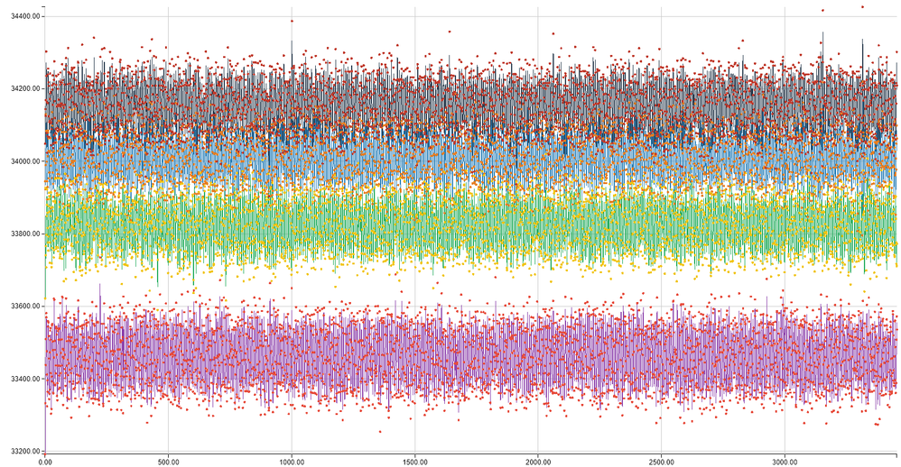
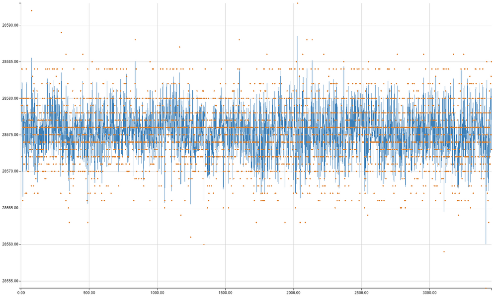
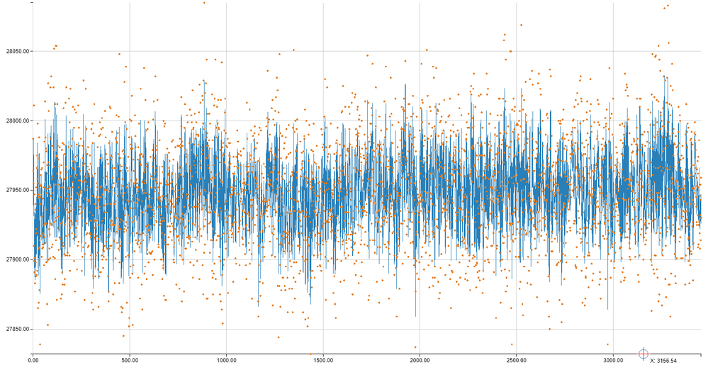
Here is actual sampled data on a channel (orange dots - actual samples, blue line - is a spline interpolation):
It looks like aliasing with higher frequency interference (sampling here is 1.333 Mhz per channel, accordingly ADC triggered at double of that - 2.666Mhz).
You got to be careful when trying to get measurements like this. Here how it looks when I am holding with my fingers the insulated wires to the capacitor that is being measured:
Next steps are:
- Try dedicated supply LDO for AVDD/VRef.
- EMI shielding (I have it all assembled in the 3D printed enclosure which I will try paint with MG Chem Super Shield). This will not save me from internal EMI emissions by STM32H7 itself.
- Y to V revision update brings some good improvements. Errata doc mentions some problems with simultaneous ADC conversation - I did not check that yet (had two ADC modules sampling simultaneously during all experiments above)
- I am committed to nail it down and get the spec-ed performance. But a bit worried for BGA100 package that I was planning to use in final 4-layer board design. It does NOT have Vref input which is my current suspect of all problems! Only AVDD pin which has Vref hooked up internally, so heavy simultaneous use of analog circuitry may deteriorate sampling.
- STM32H743 QUADSPI two independent bank operation example code in STM32 MCUs Products
- stm32h743 HAL PClock1 Calculation in STM32 MCUs Embedded software
- [STM32H7] CORTEX_M7 configuration for MPU in CUBEMX in STM32 MCUs Products
- Using -include file GCC option causes errors. in STM32CubeIDE (MCUs)
- stm32h743: Reduce Current consumption in STM32 MCUs Products
