- STMicroelectronics Community
- STM32 MCUs
- STM32 MCUs Boards and hardware tools
- STM32L412RBT, IO damaged very easily?
- Subscribe to RSS Feed
- Mark Topic as New
- Mark Topic as Read
- Float this Topic for Current User
- Bookmark
- Subscribe
- Mute
- Printer Friendly Page
STM32L412RBT, IO damaged very easily?
- Mark as New
- Bookmark
- Subscribe
- Mute
- Subscribe to RSS Feed
- Permalink
- Email to a Friend
- Report Inappropriate Content
2019-01-31 05:15 AM
Hi,
I'm using STM32L412RBT, LQFP64pin.
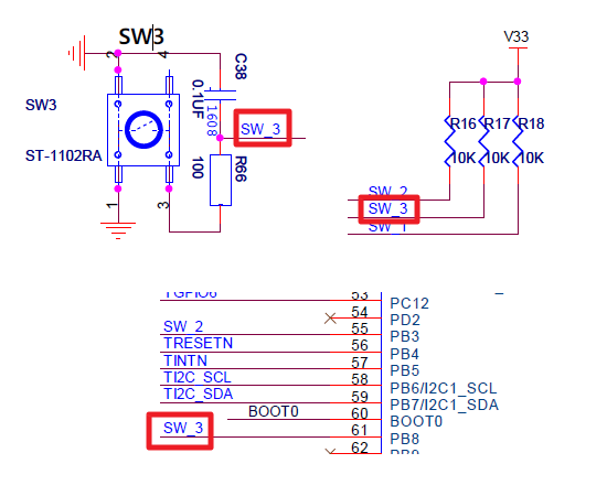
As the attached schematic, we are using some GPIO's as BTN inputs.
But, unfortunately, the GPIO got damaged very easily without special reason.
The pin voltage stuck at 1.0 ~ 1.7V when the button is not pressed.
We assembled 10 boards, and 3MCUs has this problem.
We had used the similar schematic with STM32F201, STM32F767, and so on.
But, this is the first time we're using STM32L412RBT and now we have problem.
As I know, STM32L412 is one of most recently released MCU from ST.
Is there any known issue regarding to GPIO damage ?
Or is there special design guide for STM32L412 ?
* If you want, I can send one or two MCUs for your analysis.
* If there is any known issue, I need to change the MCU to a compatible one.
* IO damage occurs on MCU RESET input pins also.
VDD is 3.3V.
Best Regards,
Danny
- Labels:
-
GPIO-EXTI
-
STM32L4 Series
- Mark as New
- Bookmark
- Subscribe
- Mute
- Subscribe to RSS Feed
- Permalink
- Email to a Friend
- Report Inappropriate Content
2019-01-31 05:39 AM
Hello @taz1000
You can contact your FAE for analyze this issue.
Kind Regards,
Imen
Thanks
Imen
- Mark as New
- Bookmark
- Subscribe
- Mute
- Subscribe to RSS Feed
- Permalink
- Email to a Friend
- Report Inappropriate Content
2019-01-31 11:50 AM
Hi @Imen DAHMEN ,
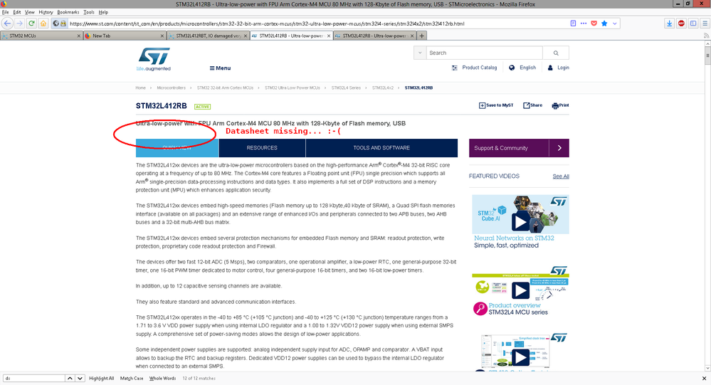
There is no datasheet at https://www.st.com/content/st_com/en/products/microcontrollers/stm32-32-bit-arm-cortex-mcus/stm32-ultra-low-power-mcus/stm32l4-series/stm32l4x2/stm32l412rb.html .
Jan
- Mark as New
- Bookmark
- Subscribe
- Mute
- Subscribe to RSS Feed
- Permalink
- Email to a Friend
- Report Inappropriate Content
2019-02-01 12:35 AM
Hi @Community member ,
You are right, I already raised internally this error for a fix.
Note, Datasheet is accessible from STM32L412CB or other product pages.
Kind Regards,
Imen.
Thanks
Imen
- Mark as New
- Bookmark
- Subscribe
- Mute
- Subscribe to RSS Feed
- Permalink
- Email to a Friend
- Report Inappropriate Content
2019-02-01 01:22 AM
I suppose the question I would be asking is why this happens on SW3, but not on SW2. (I assume they have similar external circuits).
And looking at the data sheet, I see that PB8 for SW3 has an I/O structure of FT_f whereas PB3 for SW2 has an I/O structure of FT_a.
What's the difference? They're both 5V-tolerant. But FT_f isn't something I have seen on stm32f7. It seems to be a new structure intended to allow the pin to be used for I2C at 1 MHz.
I don't see an errata document for stm32l41x, so maybe this is a fairly new family for which ST are still preparing the document. Also I see in the data-sheet, Table 19 current characteristics has a different line for FT_f maximum sink current, but the same absolute-maximum value. And in table 70, the FT_f pins can sink much harder when in FM+ mode.
So my next question is should FT_f pins be treated differently?
Is it a weakness in ST's circuit-design?
Do you ever (even at start-up or during production-testing or as a transient when setting up the pins) set PB8 as an output?
How (I didn't see it glancing through the reference manual) does one select FM+ mode for FT_f pins? Is it possible these pins are accidentally ending up in that state.
But yes, I think your next step is to contact your FAE.
Hope this helps,
Danish
- Mark as New
- Bookmark
- Subscribe
- Mute
- Subscribe to RSS Feed
- Permalink
- Email to a Friend
- Report Inappropriate Content
2019-02-01 03:43 PM
The 'L422 errata mention PB8, in a weird context of 48-pin SMPS package, which in turn is missing in the 'L422 DS... The 'L422 is most probably the same silicon die as the 'L412, only with enabled crypto.
What's the behaviour of the PB8 pin during reset, i.e. when NRST is grounded?
Is the PB8 behaviour as if a cca 10kOhm pulldown be enabled, i.e. if you change the external pullup, does the output voltage follow linearly?
JW
- Mark as New
- Bookmark
- Subscribe
- Mute
- Subscribe to RSS Feed
- Permalink
- Email to a Friend
- Report Inappropriate Content
2019-02-05 09:15 AM
The errata item about PB8 is not related to functional limitation, but to the fact this GPIO is not internally locked on 48 pin SMPS package on both L412 and L422, regardless the package is supported by the given sales type (but you are right, L422 errata needs an update to remove this item).
What is the GPIO configuration, what is the content of GPIOB registers ? (MODER, PUPDR) ?
- Mark as New
- Bookmark
- Subscribe
- Mute
- Subscribe to RSS Feed
- Permalink
- Email to a Friend
- Report Inappropriate Content
2019-02-05 09:19 AM
FM+ is enabled inside SYSCFG_CFGR1.
- Mark as New
- Bookmark
- Subscribe
- Mute
- Subscribe to RSS Feed
- Permalink
- Email to a Friend
- Report Inappropriate Content
2019-02-07 05:07 PM
All button input pins are configured to be
input mode
no pull-up, no pull-down
- Mark as New
- Bookmark
- Subscribe
- Mute
- Subscribe to RSS Feed
- Permalink
- Email to a Friend
- Report Inappropriate Content
2019-02-08 02:03 AM
Did you verify this by actually reading out the content of relevant GPIO registers?
JW

