- STMicroelectronics Community
- STM32 MCUs
- STM32 MCUs Boards and hardware tools
- Re: STM32L151C6 SWD issue
- Subscribe to RSS Feed
- Mark Topic as New
- Mark Topic as Read
- Float this Topic for Current User
- Bookmark
- Subscribe
- Mute
- Printer Friendly Page
STM32L151C6 SWD issue
- Mark as New
- Bookmark
- Subscribe
- Mute
- Subscribe to RSS Feed
- Permalink
- Email to a Friend
- Report Inappropriate Content
2015-03-17 2:42 PM
Greeting,
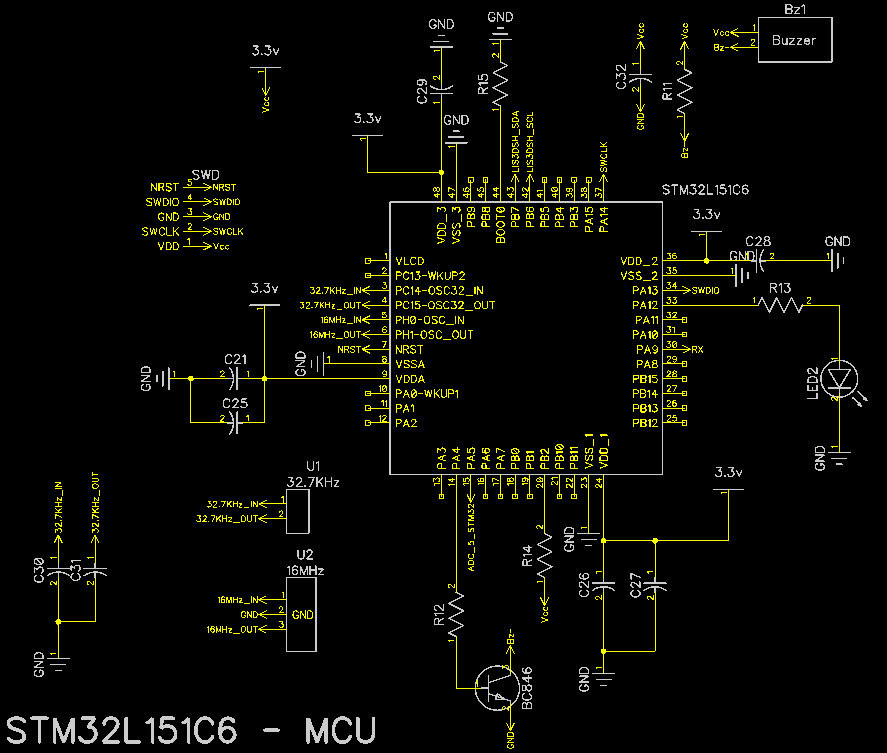
I'm facing an issue while trying to program STM32L151C6 using STM32F4 Discovery board as programmer. What I did are the following:1. I removed CN3 jumpers from STM32F4 Discovery board page 14 in [][1]2. I connect NRST, SWDIO, GND, SWCLK, Vdd to my target STM32L151C6 SWD pins except SWO ( I kept it floating)Pin:number CN2 (STM32L151C6) Pin:1 Vdd Pin:2 SWCLK (PA14) Pin:3 GND Pin:4 SWDIO (PA13) Pin:5 NRST (NRST) Pin:6 SWO (No Contact)
3. I used STM32 ST-Link Utility V2.2.6 to test SWD.The result is ''Cannot connect to ST-Link''I've attached the schematic for my circuit design.I really appreciate your prompt help guys to facilitate this issue. #swd #st-link/v2 #stm32l151c6
- Labels:
-
DEBUG
-
ST-Link
-
STM32L1 Series
- Mark as New
- Bookmark
- Subscribe
- Mute
- Subscribe to RSS Feed
- Permalink
- Email to a Friend
- Report Inappropriate Content
2015-03-17 3:41 PM
I'm not sure if that error means it can't see the ST-LINK, or the chip attached to it. If you go back to the F4 settings, does that work immediately.
Is the VDD connection necessary, or is it powering your board? Is the part correctly orientated?Up vote any posts that you find helpful, it shows what's working..
- Mark as New
- Bookmark
- Subscribe
- Mute
- Subscribe to RSS Feed
- Permalink
- Email to a Friend
- Report Inappropriate Content
2015-03-17 4:11 PM
Hi Clive,
The part is oriented correctly I double checked it. Regarding Vdd I do have power from my pcb battery (Vcc = 3.3V) I'm just following the SWD connection that's why i kept it connected to Vdd. should I remove it?I've tested the ST-Linkv2 which is provided from STM32F4 Discovery board and it's working fine with its attached STM32F4 MCU but once I disconnect the CN3 jumpers and make the connection to SWD in my PCB I got this error message.Appreciate your kind advice- Mark as New
- Bookmark
- Subscribe
- Mute
- Subscribe to RSS Feed
- Permalink
- Email to a Friend
- Report Inappropriate Content
2015-03-18 2:12 AM
Hello alharthi.waleed,
I'm using the ST-Link/V2 myself on a custom PCB and it works fine.Your SWD setup looks correct except for one part that makes me suspicious:VDD->VccThe SWD interface does not provide means to power the MCU, but it does take the MCU VDD as an input. You need to provide a power supply for the MCU from elsewhere (as you wrote, you use a battery).Not sure what Vcc voltage is since you run it over a resistor, but the SWD VDD should be connected directly to the MCU VDD (3V3).From the ST-Link/V2 documentation:''The power supply from the application board is connected to the ST-LINK/V2 debugging and programmingboard to ensure signal compatibility between both boards.''Here is some documentation on the ST-Link/V2 (check out p. 12):http://www.st.com/st-web-ui/static/active/en/resource/technical/document/user_manual/DM00026748.pdf- Mark as New
- Bookmark
- Subscribe
- Mute
- Subscribe to RSS Feed
- Permalink
- Email to a Friend
- Report Inappropriate Content
2015-03-18 7:07 AM
Hi Daniel,
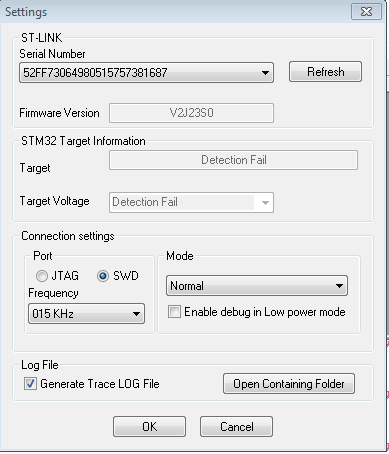
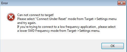
I've checked the power and it's fine there is no drop in voltages however once I tried to connect with STM32 ST-LINK Utility with the below configurations: I got below error message:
- Mark as New
- Bookmark
- Subscribe
- Mute
- Subscribe to RSS Feed
- Permalink
- Email to a Friend
- Report Inappropriate Content
2015-03-18 7:09 AM
You would only need to connect the GNDs between two independently powered systems.
I'd look at the firmware on the ST-LINK, and check if any of the solder bridges related to NRST, etc need to be removed from the DISCO board.Up vote any posts that you find helpful, it shows what's working..
- Mark as New
- Bookmark
- Subscribe
- Mute
- Subscribe to RSS Feed
- Permalink
- Email to a Friend
- Report Inappropriate Content
2015-03-18 7:15 AM
From the ST-Link/V2 documentation:
''The power supply from the application board is connected to the ST-LINK/V2 debugging and programming board to ensure signal compatibility between both boards.''
That's for the stand-alone ST-LINK/V2 which has buffering chips between the signals, the DISCO board implementation has the signals come directly out the F103 to the pins. In this context the power is derivied from the USB supply and feed to the target board, if the target board is self powered at 3.0 or 3.3V the signal levels will be compatible, and a common ground provides a path for the current/electrons.Up vote any posts that you find helpful, it shows what's working..
- Mark as New
- Bookmark
- Subscribe
- Mute
- Subscribe to RSS Feed
- Permalink
- Email to a Friend
- Report Inappropriate Content
2015-04-08 12:18 PM
First of all I would like to thank each one of you guys. I found the problem which is related to the STM32F4Discovery board I was trying to use it as a programmer. but there were issues not easy to grasp in order to modify the disco board.
What i've done was that I bought a new ST-Link-V2 and it works like charm :) without any changes to the circuit design.
Cheers, Waleed
- Mark as New
- Bookmark
- Subscribe
- Mute
- Subscribe to RSS Feed
- Permalink
- Email to a Friend
- Report Inappropriate Content
2016-01-31 9:15 AM
Hi, I'm having the same problem as yours. I made my custom board using STM32L476RET6. The programmer is the ST-Link/V2-1 from STM32L4-Discovery board. Below is my connections.
Custom board Discovery board VDD -------------------------- 3.3V SWCLK ---------------------- SWCLK GND ------------------------- GND SWDIO ---------------------- SWDIO NRST -------------------------NRST The BOOT0 pin is pulled down by 150 ohms. The jumpers on CH3 of the Discovery board are already removed. I'm successfully using the SWD of the Discovery board to program another discover board by simply connect those 6 pins of SWD ports together. However, when I tried to program my custom board, I got the same message as yours. I have checked that the clock and data signals are available on the target pins by using an oscilloscope. I really have no idea what is happening to me right now. What is the programmer are you using and where did you buy it? This is my very first comment and I cannot find the comment button in this forum. I only see reply button which seems to reply to specific comment. Regards- Mark as New
- Bookmark
- Subscribe
- Mute
- Subscribe to RSS Feed
- Permalink
- Email to a Friend
- Report Inappropriate Content
2016-01-31 10:08 AM
See ''New'' top left corner of the list of postings.
Without seeing your schematics, guessing you don't have the supplies connected correctly. Check VDDA, and scope what NRST is doing.Up vote any posts that you find helpful, it shows what's working..
- STM32U0 TIM15 clock discrepancy between Reference Manual and STM32Cube in STM32 MCUs Products
- NUCLEO-WBA65RI Phy_802_15_4 example code issue in STM32 MCUs Wireless
- STM32wb55 does not show connected even if connected to the phone in STM32 MCUs Wireless
- STM32CubeIDE 1.18.0 live expressions stopped working completely in STM32CubeIDE (MCUs)
- Issues when generating a ML inference project for the Nucleo STM32N657 in STM32CubeIDE (MCUs)