- STMicroelectronics Community
- Product forums
- ST25 NFC/RFID tags and readers
- ST25R95 - RF matching component selection, accordi...
- Subscribe to RSS Feed
- Mark Topic as New
- Mark Topic as Read
- Float this Topic for Current User
- Bookmark
- Subscribe
- Mute
- Printer Friendly Page
ST25R95 - RF matching component selection, according to my drawing of NFC antenna/coil
- Mark as New
- Bookmark
- Subscribe
- Mute
- Subscribe to RSS Feed
- Permalink
- Email to a Friend
- Report Inappropriate Content
2020-06-22 06:16 PM
Hi all.
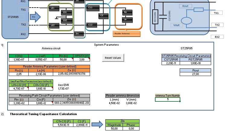
I am going to make a complete prototype of a PCB which include NFC transceiver ST25R95. I Have calculated with ST spreadsheets the values of matching capacitors from estimated values of Rant and Lant, Cant is unknown and is not being considered. The measures, I mean from one hole to another hole, the coil/antenna. The coil is drawn on both sides of the PCB.
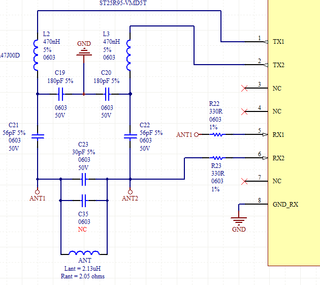
Current schematic of RF part:
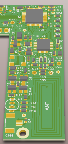
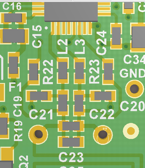
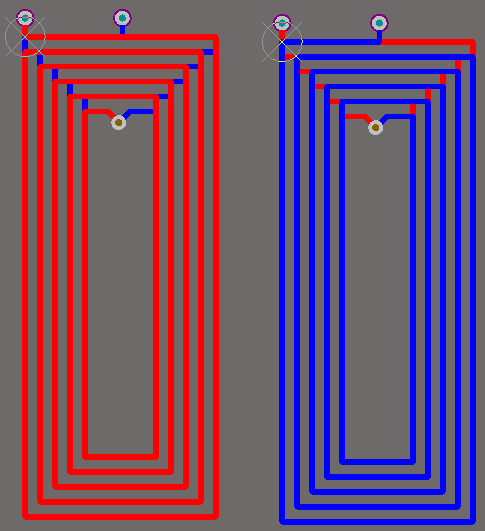
Current PCB layout:
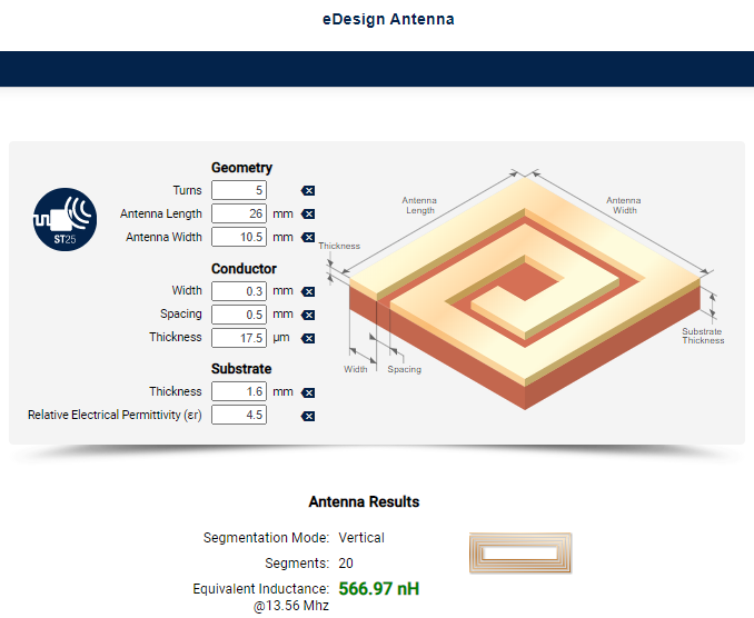
eDesign tool gives Lant = 567nH. Since the coil is double side, multiply it by 4 (but I will use 3.75). Then, 3.75 * 567nH = 2.13uH.
So I drawn the coil. Total lenght is 594mm, if consider both sides summed. Rant calculated = 2.05 ohms. To reach 2.05 ohms, use PCB parameters: 0.5 oz (18um) copper thickness, length = 594mm total and 12 mils for trace width.
Having Rant = 2.05 ohms and Lant = 2.13uH, I can use the component calculator spreadsheet of ST25R95. And from here came my values shown at the top of the topic for capacitors C21, C22 and C23.
Is there something missing on the calculations or on the procedure? For example I don't know how to calculate the capacitance between the holes, maybe it should be considered...
PCB thickness is 1.6mm.
And on layout software the antenna looks like this:
Considering that antenna, could I choose more suitable values than the ones that are currently choosen?
Regards.
Solved! Go to Solution.
Accepted Solutions
- Mark as New
- Bookmark
- Subscribe
- Mute
- Subscribe to RSS Feed
- Permalink
- Email to a Friend
- Report Inappropriate Content
2020-06-25 05:05 AM
Hello,
the procedure you followed is the right one.
just for commentsing:
- your antenna coil extraction from one layer to 2 layer is right except that multiplying the single layer coil inductance by 4 correcponds to ideal case of coupling factor between layers is 1. Generally, the signle layer coil inductance shall be multiplied by something between 3 and 4. this leads to a range of compionent values instead of fixed ones.
- Edesign suite antenna modules calculates the coil inductance taking into account the parasitic cap. thus, value given by eDesign suite is closer to the equivalent inductance extracted from imaginary part of impedance rather than the pure self inductance. so no need to hole to home capacitance.
- last point, as described in AN5248 calculated components shall be validated by a tuning circuit input impedance session.
feel free to tell us if you need help for this.
Best regards,
Henry Crane
NFC/RFID technical support
- lis2dh12 configuration settings for the lowest power consumption in MEMS (sensors)
- Confusing use of decimal separator/thousands separator in doc in STM32 MCUs TouchGFX and GUI
- Cell selection at 100 to 300mAh, Li ion, Li Polymer or LiFePO4 in STM32 MCUs Wireless
- usb otg voltage level shifter in STM32 MCUs products
- Board Selection Menu in STM32CubeIDE (MCUs)
