- STMicroelectronics Community
- STM32 MCUs Software development tools
- STM32CubeMX (MCUs)
- Configuring Timer3 for capture Compare input with ...
- Subscribe to RSS Feed
- Mark Topic as New
- Mark Topic as Read
- Float this Topic for Current User
- Bookmark
- Subscribe
- Mute
- Printer Friendly Page
Configuring Timer3 for capture Compare input with DMA on CH4. STM32H750
- Mark as New
- Bookmark
- Subscribe
- Mute
- Subscribe to RSS Feed
- Permalink
- Email to a Friend
- Report Inappropriate Content
2022-09-24 9:49 PM
After attempting to code it up myself and after it didn't work attempted to verify using CubeMX.
I have 2 questions:
- CubeMX does not give me the ability to select Alternate Function 2 on GPIOB pin 1 as input for TIM3_CH4, while Datasheet - STM32H750VB STM32H750ZB STM32H750IB STM32H750XB - 32-bit Arm® Cortex®-M7 480MHz MCUs, 128 Kbyte Flash, 1 Mbyte RAM, 46 com. and analog interfaces, crypto States PORTB alternate function does connect to TIM3_CH4 for AF2. Is this correct should TIM3 be able to do capture compare off PORTB_PIN1, or did I miss something?
- After doing HAL_TIM_IC_Start_DMA, I see the DMA copy TIM3->CCR4 to the destination (in memory) continuously even before any edge input comes in on PORTB_PIN1. Is additional synchronization needed or should this work as I expect after a __HAL_LINKDMA?
Solved! Go to Solution.
- Labels:
-
DMA
-
STM32CubeMX
-
STM32H7 series
Accepted Solutions
- Mark as New
- Bookmark
- Subscribe
- Mute
- Subscribe to RSS Feed
- Permalink
- Email to a Friend
- Report Inappropriate Content
2022-09-25 7:49 AM
1.
i try : H750VB , Tim3-CH4 capture ->
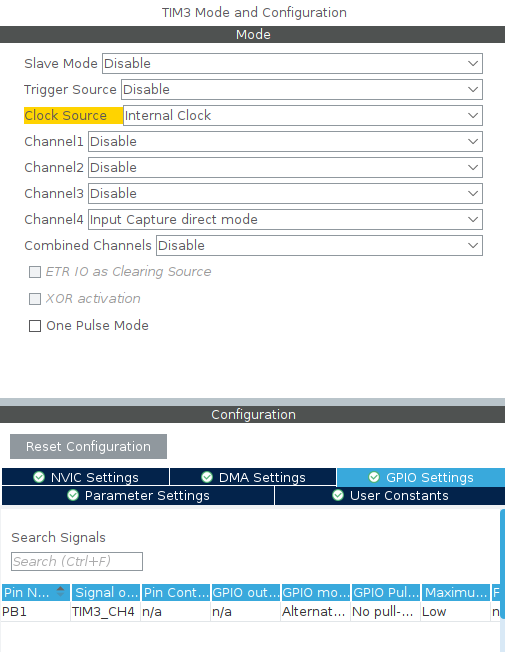
2.
what signal triggers the DMA transfer ?
- Mark as New
- Bookmark
- Subscribe
- Mute
- Subscribe to RSS Feed
- Permalink
- Email to a Friend
- Report Inappropriate Content
2022-09-25 7:49 AM
1.
i try : H750VB , Tim3-CH4 capture ->

2.
what signal triggers the DMA transfer ?
- Mark as New
- Bookmark
- Subscribe
- Mute
- Subscribe to RSS Feed
- Permalink
- Email to a Friend
- Report Inappropriate Content
2022-09-26 10:59 AM
Hi AScha.3
Thanks for checking CubeMX, it looks like I needed to put PINB_1 into AF2_TIM3_CH4 before the other UI would recognize and use PB1.
Regarding your question about the trigger, I'm actually unsure what it is triggering on currently, the mux seems to be setup for CH4 output (code below). What I want it to trigger on is: both edges of the signal on PB1 input capture (the input signal is about 1Mhz). So on both edges I want the DMA to capture the (tim3) counter value and write it into a buffer in sram, while incrementing the offset.
#define SRAM1_DATA __attribute__((section(".sram1_bss")))
SRAM1_DATA uint16_t SDataBuffer[160];
TIM_ClockConfigTypeDef sClockSourceConfig = {0};
TIM_MasterConfigTypeDef sMasterConfig = {0};
TIM_IC_InitTypeDef sConfigIC = {0};
TIM_SlaveConfigTypeDef sSlaveConfig = {0};
htim3.Instance = TIM3;
htim3.Init.Prescaler = 0;
htim3.Init.CounterMode = TIM_COUNTERMODE_UP;
htim3.Init.Period = 65535;
htim3.Init.ClockDivision = TIM_CLOCKDIVISION_DIV1;
htim3.Init.AutoReloadPreload = TIM_AUTORELOAD_PRELOAD_DISABLE;
if (HAL_TIM_Base_Init(&htim3) != HAL_OK)
{
Error_Handler();
}
sClockSourceConfig.ClockSource = TIM_CLOCKSOURCE_INTERNAL;
if (HAL_TIM_ConfigClockSource(&htim3, &sClockSourceConfig) != HAL_OK)
{
Error_Handler();
}
if (HAL_TIM_IC_Init(&htim3) != HAL_OK)
{
Error_Handler();
}
sMasterConfig.MasterOutputTrigger = TIM_TRGO_ENABLE;
sMasterConfig.MasterSlaveMode = TIM_MASTERSLAVEMODE_DISABLE;
if (HAL_TIMEx_MasterConfigSynchronization(&htim3, &sMasterConfig) != HAL_OK)
{
Error_Handler();
}
sConfigIC.ICPolarity = TIM_INPUTCHANNELPOLARITY_BOTHEDGE;
sConfigIC.ICSelection = TIM_ICSELECTION_DIRECTTI;
sConfigIC.ICPrescaler = TIM_ICPSC_DIV1;
sConfigIC.ICFilter = 0;
if (HAL_TIM_IC_ConfigChannel(&htim3, &sConfigIC, TIM_CHANNEL_4) != HAL_OK)
{
Error_Handler();
}
GPIO_InitTypeDef GPIO_InitStruct = {0};
HAL_DMA_MuxSyncConfigTypeDef pSyncConfig;
__HAL_RCC_TIM3_CLK_ENABLE();
GPIO_InitStruct.Pin = GPIO_PIN_1;
GPIO_InitStruct.Mode = GPIO_MODE_INPUT;
GPIO_InitStruct.Pull = GPIO_PULLUP;
GPIO_InitStruct.Speed = GPIO_SPEED_FREQ_LOW;
GPIO_InitStruct.Alternate = GPIO_AF2_TIM3;
HAL_GPIO_Init(GPIOB, &GPIO_InitStruct);
hdma_tim3_ch4.Instance = DMA1_Stream5;
hdma_tim3_ch4.Init.Request = DMA_REQUEST_TIM3_CH4;
hdma_tim3_ch4.Init.Direction = DMA_PERIPH_TO_MEMORY;
hdma_tim3_ch4.Init.PeriphInc = DMA_PINC_DISABLE;
hdma_tim3_ch4.Init.MemInc = DMA_MINC_ENABLE;
hdma_tim3_ch4.Init.PeriphDataAlignment = DMA_PDATAALIGN_HALFWORD;
hdma_tim3_ch4.Init.MemDataAlignment = DMA_MDATAALIGN_HALFWORD;
hdma_tim3_ch4.Init.Mode = DMA_CIRCULAR;
hdma_tim3_ch4.Init.Priority = DMA_PRIORITY_LOW;
hdma_tim3_ch4.Init.FIFOMode = DMA_FIFOMODE_ENABLE;
hdma_tim3_ch4.Init.FIFOThreshold = DMA_FIFO_THRESHOLD_FULL;
hdma_tim3_ch4.Init.MemBurst = DMA_MBURST_SINGLE;
hdma_tim3_ch4.Init.PeriphBurst = DMA_PBURST_SINGLE;
if (HAL_DMA_Init(&hdma_tim3_ch4) != HAL_OK)
{
Error_Handler();
}
__HAL_RCC_DMA1_CLK_ENABLE();
__HAL_LINKDMA(&htim3, hdma[TIM_DMA_ID_CC4], hdma_tim3_ch4);
HAL_TIM_IC_Start_DMA(&htim3, TIM_CHANNEL_4, (uint32_t*)&(SDataBuffer[0]), sizeof(SDataBuffer) / sizeof(SDataBuffer[0]));
// GPIOC_PIN4 is connected to GIOPB_PIN1 for test purposes.
while (1) {
GPIOC->BSRR = (1 << 4) << 16;
volatile uint32_t x = 540;
while (x--) {}
GPIOC->BSRR = (1 << 4);
x = 540;
while (x--) {}
}
- Mark as New
- Bookmark
- Subscribe
- Mute
- Subscribe to RSS Feed
- Permalink
- Email to a Friend
- Report Inappropriate Content
2022-09-27 11:41 PM
@AScha.3 It would help to know, whether I should be able to do capture of the timer through DMA on TIM3_CH4 input. Without any more CPU interaction.
- Mark as New
- Bookmark
- Subscribe
- Mute
- Subscribe to RSS Feed
- Permalink
- Email to a Friend
- Report Inappropriate Content
2022-09-28 4:06 AM
Well, should be possible . :) but is not easy, to adjust complex timer to this...
how many data you want to collect ? at frequency xx ? because at us range it will be many data in short time...
or write DMA to circular buffer ?
just: what you want to do with this ?
i made an IR receiver , decoding the IR remote signal, with interrupt after every full pulse;
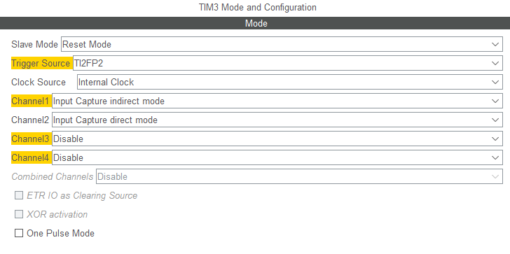
about this way (just on CH 3+4) it should work:

- Mark as New
- Bookmark
- Subscribe
- Mute
- Subscribe to RSS Feed
- Permalink
- Email to a Friend
- Report Inappropriate Content
2022-09-28 9:07 AM
@AScha.3
>> just: what you want to do with this ?
I'm attempting to time the polarity changes on PinB_1 which are encoded bits based on pulse width. I want to offload the timing from the CM7, with a maximum transfer size being 10 bytes. At maximum: 10 * 8 * 2 = 160 captures (2 edges per bit) this way the CM7 can defer handling the data instead of missing it or having to interrupt something else important.
I do not have IOs left that connect to any CH1/CH2 combo and TIM3_CH4 (on PB1) seems to be the only pin that I have left connecting to a timer.
The timing is 4us per bit, 1us minimum pulse width.
After enabling the "internal clock" on the timer through Cube, I now do not see the DMA occurring at all.
I also do not see the CCR4 register change, while I know the signal on PB1 is changing (verified through a logic analyzer).
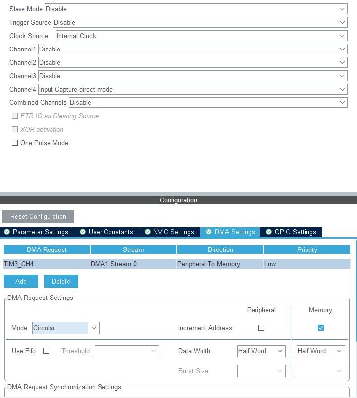
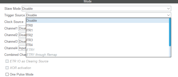
TIxFPy seem to all need a second IO pin which I do not have. Is there any way around this?
- Mark as New
- Bookmark
- Subscribe
- Mute
- Subscribe to RSS Feed
- Permalink
- Email to a Friend
- Report Inappropriate Content
2022-09-28 10:07 AM
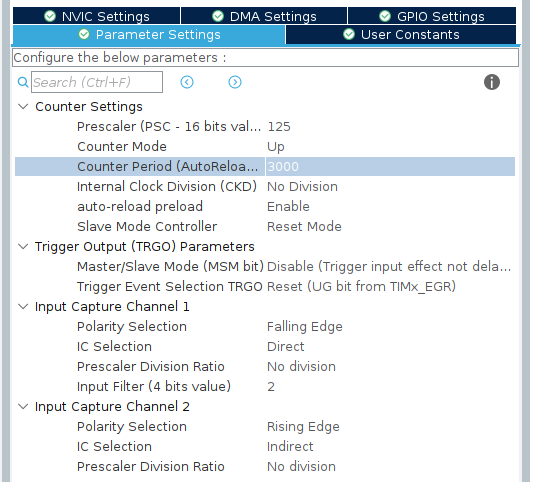
ok, so YOU take CH3/4 for capture , just i took CH1/2 because only this free pins - to show you, how to.
+ yes, slave mode -> then set Trigger source ; so it only starts timer on trigger (here from the pin -> TI_FP_ ). other wise timer runs always, what we obviously do not want here.
+ look, what i select exactly! direct/indirect mode...combination, so you get hi-time in a capture and lo-time in other channel of one complete pulse on one input pin !
+ set clock/divider to useful value, maybe 100MHz , so you get 400 at 4us pulse and counter period 500, so timer ends capture on any wrong pulse after 5us.
see my setting , also rising/falling edge selection...
- Mark as New
- Bookmark
- Subscribe
- Mute
- Subscribe to RSS Feed
- Permalink
- Email to a Friend
- Report Inappropriate Content
2022-09-28 12:58 PM
This was all I needed actually. (AScha.3 first comment)
Most important things I missed was the Clock Source needing to be set to "Internal Clock" and PB1 being initialized to TIM3_CH4.
Additionally, I goofed on the PB1 pin setup internally, and set it to GPIO_MODE_INPUT instead of GPIO_MODE_AF_OD which took me for a loop.
The suggested trigger source was unnecessary for my application as that only starts the timer, in my case TI1/2_FP1/2 could not be used as it needed an additional GPIO input.
For me having the timer free-running is not an issue as long as both edges on IC CH4 trigger a DMA transfer from CCR4 to a circular buffer. I can calculate the delta between the captures in my code.
I have not fully grokked how to apply indirect mode to my signal yet, but that also seems possible in with CH3 should be set to indirect and counter mode to Center Aligned.
- STM32CubeMX with MMT: strange LD file generation in STM32CubeMX (MCUs)
- BUG FOUND IN LTDC 18bits mode in STMCubeMX 6.15.0 in STM32CubeMX (MCUs)
- [bugs/caveats/misc fixes] STM32H7S Cube in STM32CubeMX (MCUs)
- Output compare mode. in STM32CubeIDE (MCUs)
- Timer - Conflict between ETR1 and Output Compare on CH1? in STM32CubeMX (MCUs)