- Subscribe to RSS Feed
- Mark Topic as New
- Mark Topic as Read
- Float this Topic for Current User
- Bookmark
- Subscribe
- Mute
- Printer Friendly Page
TIMER
- Mark as New
- Bookmark
- Subscribe
- Mute
- Subscribe to RSS Feed
- Permalink
- Email to a Friend
- Report Inappropriate Content
2023-10-30 02:45 AM
Hello,
I found an example on the internet of a project but I don't understand the usefulness of using a Timer 7. Could you tell me why ? Thanks in advance.
__IO uint32_t usTick;
void HAL_TIM_PeriodElapsedCallback(TIM_HandleTypeDef *htim)
{
  /* Prevent unused argument(s) compilation warning */
  if(htim==&htim7){
	usTick++;
	}
  /* NOTE : This function Should not be modified, when the callback is needed,
            the __HAL_TIM_PeriodElapsedCallback could be implemented in the user file
   */
}

void delay_us(__IO uint32_t Delay){
uint32_t t=usTick;
uint32_t wait = Delay;
while( usTick - t < wait);

}
int main(void)
{

  /* Reset of all peripherals, Initializes the Flash interface and the Systick. */
  HAL_Init();

  /* Configure the system clock */
  SystemClock_Config();

  /* Initialize all configured peripherals */
  MX_GPIO_Init();
  MX_TIM7_Init();
	/*if (HAL_TIM_Base_Start(&htim7) != HAL_OK) {
		      _Error_Handler(__FILE__, __LINE__);
    }*/
	if (HAL_TIM_Base_Start_IT(&htim7) != HAL_OK) {
		      _Error_Handler(__FILE__, __LINE__);
    }

  MX_I2C1_Init();
	  MX_I2S2_Init();

	HAL_Delay(100);

	audio.init();


	bool ptt=HAL_GPIO_ReadPin(GPIOE,PTT_SWITCH);
	bool pttstate=ptt;
	uint16_t index = 0;
	uint16_t buf = 0;
	audio.set_volume(0);
  /* Infinite loop */
  	while (1)//	read power switch
	{
		ptt=HAL_GPIO_ReadPin(GPIO_PINS,PTT_SWITCH);
		if(ptt!=pttstate){
			if(ptt==0){

				audio.start_receive();
				for(buf=0;buf<32;buf++){
					for(index=0;index < AUDIO_BUF_SIZE;index++){
						HAL_I2SEx_TransmitReceive(&hi2s2, &i2s_zero,&i2s_buf[buf][index], 1,0xFF);
					}
				}

				audio.start_play();
				for(buf=0;buf<32;buf++){
					for(index=0;index < AUDIO_BUF_SIZE;index++){
						HAL_I2SEx_TransmitReceive(&hi2s2, &i2s_buf[buf][index],&i2s_zero, 1,0xFF);
					}
				}
			}

			pttstate=ptt;
		}
  	}

}
- Labels:
-
STM32L5 Series
- Mark as New
- Bookmark
- Subscribe
- Mute
- Subscribe to RSS Feed
- Permalink
- Email to a Friend
- Report Inappropriate Content
2023-11-03 09:01 AM
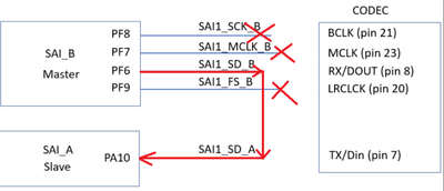
without the audio board : so no connection of SAI_SCK_B SAI1_MCLK_B and SAI1_FS_B like this :
Just only a connection between SAI1_SD_B and SAI1_SD_A ?
What do you mean 'you should see DA data in the AD buffers.' DA and AD what it's for you ? Probably Digital to Analog and Analog to Digital ?
- Mark as New
- Bookmark
- Subscribe
- Mute
- Subscribe to RSS Feed
- Permalink
- Email to a Friend
- Report Inappropriate Content
2023-11-05 10:17 PM
Yes for AD / DA.
Use both TX and RX SAI in DAM circular mode.
Start both before while loop, start slave first.
- Mark as New
- Bookmark
- Subscribe
- Mute
- Subscribe to RSS Feed
- Permalink
- Email to a Friend
- Report Inappropriate Content
2023-11-05 11:29 PM - edited 2023-11-06 05:57 AM
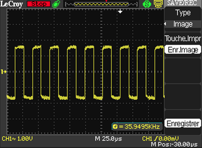
On the LRCLK pin I have a following signal :
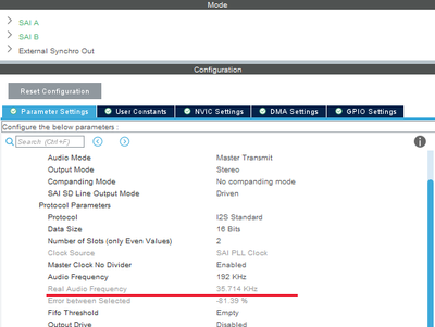
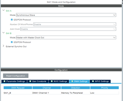
And after my configuration for the SAI (or I2S) it seems to me that it is correct :
I
I have completed the entire table but how do I check for data reception ? I have always 54 in the register CHIP_ANA_CTRL.data.
How to start DMAs (first start the slave, then the master). After my code After my code, I only started the master but not the slave, is that right ?
 HAL_SAI_RegisterCallback(&hsai_BlockB1, HAL_SAI_TX_HALFCOMPLETE_CB_ID, HAL_SAI_TxHalfCpltCallback);
  HAL_SAI_RegisterCallback(&hsai_BlockB1, HAL_SAI_TX_COMPLETE_CB_ID, HAL_SAI_TxCpltCallback);
  fresult= HAL_SAI_Init(&hsai_BlockB1);
  if (fresult != HAL_OK)
	{
  	return HAL_ERROR;
	}
  fresult = HAL_SAI_Transmit_DMA(&hsai_BlockB1, (uint8_t *)playbuf , (sizeof(playbuf))/4);
Probably I must do the same with hsai_BlockA1 ?
- Mark as New
- Bookmark
- Subscribe
- Mute
- Subscribe to RSS Feed
- Permalink
- Email to a Friend
- Report Inappropriate Content
2023-11-06 09:12 AM
As I said, BEFORE entering the while loop, in main, start the SAI-slave DMA first, then the SAI-master DMA.
In the RX complete callback you could compare DA / DA buffers, count the errors or set a flag if not equal.
- Mark as New
- Bookmark
- Subscribe
- Mute
- Subscribe to RSS Feed
- Permalink
- Email to a Friend
- Report Inappropriate Content
2023-11-07 02:00 AM - edited 2023-11-07 02:02 AM
Yes I can see your message but it's not easy for me to do 'Start the SAI-slave DMA first' ?? So I did something like this :
  HAL_SAI_RegisterCallback(&hsai_BlockA1, HAL_SAI_RX_HALFCOMPLETE_CB_ID, HAL_SAI_RxHalfCpltCallback);
  HAL_SAI_RegisterCallback(&hsai_BlockA1, HAL_SAI_RX_COMPLETE_CB_ID, HAL_SAI_RxCpltCallback);
  fresult= HAL_SAI_Init(&hsai_BlockA1);
  if (fresult != HAL_OK)
  	{
  	return HAL_ERROR;
  	}
  fresult = HAL_SAI_Receive_DMA(&hsai_BlockA1, (uint8_t *)playbuf_RX, (sizeof(playbuf_RX))/4);
No errors during compilation, but at this line :
fresult = HAL_SAI_Receive_DMA(&hsai_BlockA1, (uint8_t *)playbuf_RX, (sizeof(playbuf_RX))/4);
the code is elsewhere, there is an error in the interrupts but I don't know where it could come from ?
Do you have any idea where this could come from ?
- Mark as New
- Bookmark
- Subscribe
- Mute
- Subscribe to RSS Feed
- Permalink
- Email to a Friend
- Report Inappropriate Content
2023-11-07 02:10 AM - edited 2023-11-07 02:14 AM
I wonder why it is necessary to start the DMA of the slave? Normally it's synchronizing the SAI according to my configuration, right ?
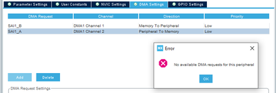
Or probably I need to add a DMA line for the slave ?
But It's not allowed
- Mark as New
- Bookmark
- Subscribe
- Mute
- Subscribe to RSS Feed
- Permalink
- Email to a Friend
- Report Inappropriate Content
2023-11-07 03:40 AM
Yes, you must activate an individual DMA for each SAI or SAI block.
So you have a DMA stream for SAI TX, and another DMA stream for SAI RX.
SAI in slave mode only refers to the clocks, so a SAI slave gets the clocks (SCLK, LRCK, (MCLK)) from either an external IC via the pins (e.g., a codec), or internally from another SAI / SAI block.
So you want to route these clocks from the SAI master internally, so activate synchronization between SAIs or blocks.
- Mark as New
- Bookmark
- Subscribe
- Mute
- Subscribe to RSS Feed
- Permalink
- Email to a Friend
- Report Inappropriate Content
2023-11-07 06:43 AM
Thank you for this information. But I would like to ask this question again because I did not understand your answer. the wiring of the assembly is as follows :
Just only a connection between SAI1_SD_B and SAI1_SD_A ? And no connection of SAI_SCK_B SAI1_MCLK_B and SAI1_FS_B.
The SAI1_SD_A : I can understand, these are the data from the ADC but the SAI1_SD_B what it's exactly ? What does the master want to convey ? Is it really necessary to make this connection ? Because I want only recover data from the sensor via the ADC.
Or I need this link to simulate data from the ADC via my playbuf array ? In this case we only check the SAI interface and nothing else ? Right ?
- Mark as New
- Bookmark
- Subscribe
- Mute
- Subscribe to RSS Feed
- Permalink
- Email to a Friend
- Report Inappropriate Content
2023-11-07 09:04 AM
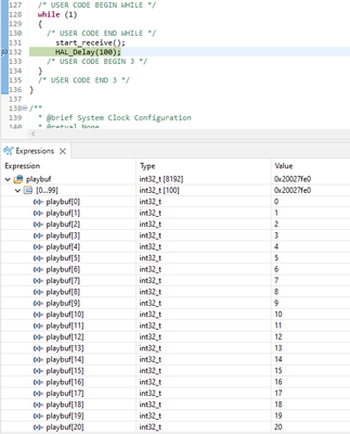
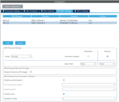
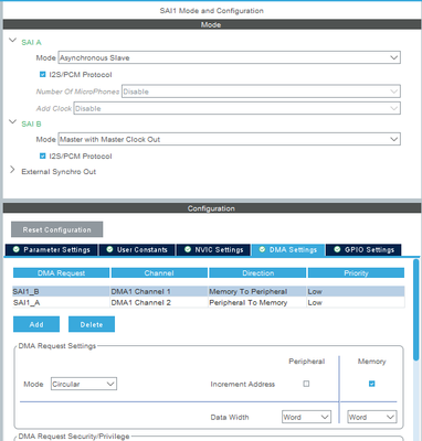
I have this configuration and I have the DMA for the master and for the slave. I'm getting some data but I'm not sure if I should get this? Does this verification method actually work ?
I have this code with the slave
  HAL_SAI_RegisterCallback(&hsai_BlockA1, HAL_SAI_RX_HALFCOMPLETE_CB_ID, HAL_SAI_RxHalfCpltCallback);
  HAL_SAI_RegisterCallback(&hsai_BlockA1, HAL_SAI_RX_COMPLETE_CB_ID, HAL_SAI_RxCpltCallback);
  fresult= HAL_SAI_Init(&hsai_BlockA1);
  if (fresult != HAL_OK)
  	{
  	return HAL_ERROR;
  	}
  fresult = HAL_SAI_Receive_DMA(&hsai_BlockA1, (uint8_t *)playbuf, (sizeof(playbuf_RX))/4);
And I wonder why have the same array (playbuf) for the TX and the RX ?
- Mark as New
- Bookmark
- Subscribe
- Mute
- Subscribe to RSS Feed
- Permalink
- Email to a Friend
- Report Inappropriate Content
2023-11-07 10:06 PM
Connections:
Yes, this is only to test the SAI functionality. But you should have that working and understand it before going further.
All the clocks between 2 SAI blocks can be connected internally, I think CubeMX - when setting a SAI to slave - has some setting like "synchronous to other SAI block" or so.
Buffers:
Your wondering is correct, using the same buffer is wrong.
Again:
You must get a clear head and understand what's going on, and what should happen...
Before connecting an ADC or DAC or Codec, you should find out out how the SAI works.
So my idea was to "simulate" DAC and ADC by connecting the SAI data lines, using a known source for the DAC/TX ("playbuf"), and a then receive the same data with the AD / RX SAI, into its own buffer ("recbuf"?).
If all is going well, both SAIs have the same data setup and are synchronized, then recbuf should be equal to playbuf.
When that is working, you hopefully have enough control over the SAI that you can start working with an external audio converter (which might need to be setup via registers and I2C, so that's another story).
I'm out for now, got some work of my own...
- Input capture / Frequency Measurement error on STM32U545REQ in STM32 MCUs Products
- Cannot Compile When using example ioc in STM32 MCUs Wireless
- STM32WLE5 Exit stop mode 2 on EXTI or RTC timer in STM32 MCUs Wireless
- Timer XOR ON / Hall Sensor Mode Edge Trigger Problem in STM32 MCUs Products
- STM32L431CBT6 blocks in HAL_Delay() in STM32 MCUs Products

