Turn on suggestions
Auto-suggest helps you quickly narrow down your search results by suggesting possible matches as you type.
Showing results for
- STMicroelectronics Community
- STM32 MCUs
- STM32 MCUs Products
- Re: How to configure FSMC for the task?
Options
- Subscribe to RSS Feed
- Mark Topic as New
- Mark Topic as Read
- Float this Topic for Current User
- Bookmark
- Subscribe
- Mute
- Printer Friendly Page
How to configure FSMC for the task?
Options
- Mark as New
- Bookmark
- Subscribe
- Mute
- Subscribe to RSS Feed
- Permalink
- Email to a Friend
- Report Inappropriate Content
2014-11-11 01:26 AM
Posted on November 11, 2014 at 10:26
Hi, All.
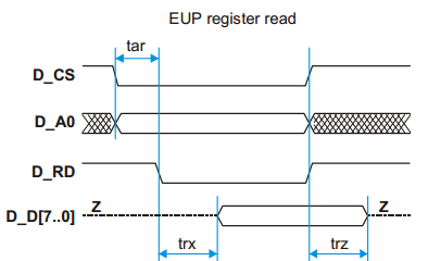
??????? ???, All! I need connect MCU to , but I can't understand, how should comfigure FSMC. I'm using STM32F407VG (then it will replaced to STM32F103VC). I have read descriptions MCU and AN2790, but it didn't help me. What I want? I have &sharpCS, &sharpWR, &sharpRD, &sharpA0 ('♯' means inverted) and D0..D7 data/adress. ST says in the AN it 8080-like type. I need NOR interface. Ok, but I still have one problem. For multiple read or write the device need 'read' ( or 'write' in second case) condition, then clean, then set 'read' again, ... I can select adress over connecting &sharpA0 of device to A9 of MCU. But how to configure FSMC for save possibility read/write miltiple values in the same register? I think about external gate for &sharpWR and &sharpRD, managed by CLK.. I very hope, it can be decided over configure FSMC., see page 11., page 48 (It isn't english!) PS: Sorry my enlish. b.r., Oleg #fsmc
Labels:
- Labels:
-
FMC-FSMC
4 REPLIES 4
Options
- Mark as New
- Bookmark
- Subscribe
- Mute
- Subscribe to RSS Feed
- Permalink
- Email to a Friend
- Report Inappropriate Content
2014-11-11 01:41 AM
Posted on November 11, 2014 at 10:41
I don't quite understand what's your problem. Try to describe it in more detail. (I do understand Russian a bit, but others here probably don't).
JWOptions
- Mark as New
- Bookmark
- Subscribe
- Mute
- Subscribe to RSS Feed
- Permalink
- Email to a Friend
- Report Inappropriate Content
2014-11-11 02:08 AM
Posted on November 11, 2014 at 11:08
I asked
. Look it, please. Maybe you catch more... And for other. So, on the picture 'read' operation from device. It can autoincremen adressing.. no. One more time - device has FIFO register, wich register - it defined by value from ADR register (select by #A0). It means, I should read values from the same adress few times without second (3-th, 4-th,...) select addres. Like burst mode, but for 'write' operation also. On the picture, after Trz I should reset #WR ( =0), read data(i+1), set #WR, and repeat that some time.
Options
- Mark as New
- Bookmark
- Subscribe
- Mute
- Subscribe to RSS Feed
- Permalink
- Email to a Friend
- Report Inappropriate Content
2014-11-11 03:25 AM
Posted on November 11, 2014 at 12:25
I still don't quite understand your problem.
Simply connect directly the /RD, /WR, /CS, data as appropriate, and address to any address pin (N). Then, accessing any address which falls into respective FSMC area and has bit N cleared accesses the address register of modem; accessing address which has bit N set accesses the data register. If you are concerned about back-to-back writes/reads, they are probably separated by 1 cycle by default (the datasheet/RM is unclear about it), and this time can be increased by setting the BUSTURN field Review the waveforms in FSMC chapter of RM0090, the timing parameters the datasheet, and have a look at [DEAD LINK /public/STe2ecommunities/mcu/Lists/cortex_mx_stm32/Flat.aspx?RootFolder=/public/STe2ecommunities/mcu/Lists/cortex_mx_stm32/memory%20with%20long%20write%20recovery%20time%20with%20FSMC%20of%20STM32F407IG&FolderCTID=0x01200200770978C69A1141439FE559EB459D7580009C4E14902C3CDE46A77F0FFD06506F5B¤tviews=712]this thread. JWOptions
- Mark as New
- Bookmark
- Subscribe
- Mute
- Subscribe to RSS Feed
- Permalink
- Email to a Friend
- Report Inappropriate Content
2014-11-11 11:17 PM
Posted on November 12, 2014 at 08:17
Thank you!
Did I read this Reference Manual esterday? Yes, of course. Few times. But didn't see waveform diagrams! Don't ask me - 'how'. I'm confused. So, I'll use Mode A and 9 pins for data-adress. The highest (A8) will use as data/adress signal.
Related Content
- STM32F0 minimal RTOS example doesn't work in STM32 MCUs Embedded software
- How to use USART2 instead of USART1 in BLE_p2pServer example? in STM32 MCUs Wireless
- STM32F401 ADC VrefInt and Vbat read issue in STM32 MCUs Products
- STM32wb55 go to sleep in standby mode but do not wake up with sequencer in STM32 MCUs Wireless
- Guidance Needed for USB Implementation with FreeRTOS on STM32F756ZG in STM32 MCUs Embedded software