- STMicroelectronics Community
- STM32 MCUs
- STM32 MCUs Products
- Re: Help needed to understand the circuits of the ...
- Subscribe to RSS Feed
- Mark Topic as New
- Mark Topic as Read
- Float this Topic for Current User
- Bookmark
- Subscribe
- Mute
- Printer Friendly Page
Help needed to understand the circuits of the x-nucleo-ihm08m1
- Mark as New
- Bookmark
- Subscribe
- Mute
- Subscribe to RSS Feed
- Permalink
- Email to a Friend
- Report Inappropriate Content
2023-09-25 4:52 AM
Hi, is there anyone who can help me to understand the circuits of the x-nucleo-ihm08m1 ? Like explaining to me how the figure 5 does the analog conditiong and current protection.
- Labels:
-
Documentation
- Mark as New
- Bookmark
- Subscribe
- Mute
- Subscribe to RSS Feed
- Permalink
- Email to a Friend
- Report Inappropriate Content
2023-09-25 7:59 AM
Hello @Gnahore ,
Could you please check the section 4 Circuit description :
user manual : Getting started with X-NUCLEO-IHM08M1 low-voltage BLDC motor driver expansion board based on STL220N6F7 for STM32 Nucleo
You can find the necessary explanation for each part.
Foued
To give better visibility on the answered topics, please click on Accept as Solution on the reply which solved your issue or answered your question.
- Mark as New
- Bookmark
- Subscribe
- Mute
- Subscribe to RSS Feed
- Permalink
- Email to a Friend
- Report Inappropriate Content
2023-09-26 7:22 AM
Hi, I have seen it already but I wanted a bit more explanation.
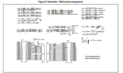
The figure 5 and figure 6 are the ones I really struggle with. Look at the figure 6. What does that mean when a wire as for label "Pin_name - Something"? Such as "PA5 - DAC". I recently learned that General Purpose I/O (GPIO) pins do not only function as input/output but can also serve alternative function which has to be set. Therefore is the word next to the Pin_name precise its function? "PA5 - DAC" means the pin 5 of port A will be set as an analog GPIO? What about "PB4 - PWM" and "PA10-WH"?
Also some wire has 2 pin names on them like "PA5/PB13". What does that mean?
Lastly the figure 5 is an analog conditioning and current protection. Can someone explain to be me how this is an analog conditioning and how this circut is a protection to overccurent ? I kinda understand the 3 circuits on the right side. These are comparators, if V_shuntX is above Vref (=0.33V) BKIN is equal to 0 however if V_shuntX is below Vref BKIN is equal to 3.3V. How doing this is a current protection?
- Mark as New
- Bookmark
- Subscribe
- Mute
- Subscribe to RSS Feed
- Permalink
- Email to a Friend
- Report Inappropriate Content
2023-09-26 8:02 AM
I don't know the rest of the circuit, but I guess:
No current protection there, but amplifiers and comparators for monitoring the currents, so that the MCU can react.
Figure 5, left side:
these are simple non-inverting amplifiers, probably for amplifying the low voltage signals (because of low ohmic shunts, U = R * I ...) from the power MOSFETs' shunts
right side:
comparators, probably connected to GPIOs to trigger an interrupt in case of overcurrent = voltage over shunts too high
- Mark as New
- Bookmark
- Subscribe
- Mute
- Subscribe to RSS Feed
- Permalink
- Email to a Friend
- Report Inappropriate Content
2023-09-27 4:37 AM - edited 2023-09-27 4:38 AM
Hello,
Ok so there are non-inverting amplifiers. Are curr_dbk[3:1] currents ?
Based on the reference manual BKIN serves as emergency shut-down of PWM signals. BKIN shut down PWM signals when the ouput of the comparators are at 0 or 3v3?
Thanks for helping me
PS : I forget to add this
- Mark as New
- Bookmark
- Subscribe
- Mute
- Subscribe to RSS Feed
- Permalink
- Email to a Friend
- Report Inappropriate Content
2023-09-27 5:24 AM
You should learn the basics before fiddling with such a complex (for beginners) circuit.
curr_fdbk[3:1] probably stands for "current feedback", and as these signals are outputs of the opamps, they are voltages, probably going to the STM's ADC input so that the MOSFET currents can be measured.
The comparator output must be open collector, so by connecting them an inverse OR is created, so if one of the three pulls the signal down (0V), then BKIN is 0V, no matter what the other 2 are doing.
So probably overcurrent = 0V.
Check where BKIN is going (schematics) and what the STM is doing with that signal.
As I said, probably going to a GPIO with interrupt enabled, so that the STM32 can quickly pause / stop / whatever the PWMs.
PS: the screenshots are mostly useless because of the resolution, a link to the manual containing the schematics would be better (I found it)
- Mark as New
- Bookmark
- Subscribe
- Mute
- Subscribe to RSS Feed
- Permalink
- Email to a Friend
- Report Inappropriate Content
2023-09-27 6:25 AM - edited 2023-09-27 6:46 AM
Yes I know.. I'm in intership and I have to use these circuits as a reference to make my own (the software part of my project is done, now I work on the hardware part).
Ok I was confused because of the name.
"an inverse OR is created" what does "OR" stand for? Ok, overccurent = 0V.
I checked on the schematics and BKIN is connected to PA11, PA6 and there is another wire that says "PA6/PB14".
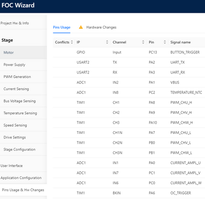
Based on the stm32f302r8 datasheet, PA6 can be used as a GPIO or 4 alternate functions which are TIM16_CH1, TSC_G2_IO3, TIM1_BKIN, EVENTOUT and 2 additional functions which are ADC1_IN10 and OPAMP2_VOUT. However, I made a project with MCSDK which generated a C code and ioc file. In the ioc file, none of these pins (PA6, PB11 or "PA6/PB14") have been set as GPIO analog + ADC1_IN10. How to interpret that then?
Also what does it mean when there is 2 pins name on the same wire like PA6/PB14? Does that mean I must make a choice?
Big apologize, I didn't realize the resolution was that bad. Here is the sources :
https://www.st.com/resource/en/datasheet/stm32f302r8.pdf (MCU datasheet)
https://www.st.com/resource/en/schematic_pack/x-nucleo-ihm08m1_schematic.pdf (x-nucleo-ihm08m1 schematic)
https://www.st.com/resource/en/reference_manual/rm0365-stm32f302xbcde-and-stm32f302x68-advanced-armbased-32bit-mcus-stmicroelectronics.pdf (stm32f302 reference manual)
EDIT : I have found that on the MCSDK
PA6 is supposedly set as BKIN but I swear, the ioc file allowed me to use it. It was in reset_state mode (grey). This is why I could made my ioc file this way :
- Mark as New
- Bookmark
- Subscribe
- Mute
- Subscribe to RSS Feed
- Permalink
- Email to a Friend
- Report Inappropriate Content
2023-09-27 6:49 AM
OR: I was a little unclear, I mean the logic "or" function
BKIN is a comparator output, so no need for analog / ADC. It's either high or low.
I would have guessed ST uses that as an interrupt source to react quickly, but maybe it's used for polling.
When you are doing an internship, then you should mainly ask your supervisor, or whatever that's called.
- Mark as New
- Bookmark
- Subscribe
- Mute
- Subscribe to RSS Feed
- Permalink
- Email to a Friend
- Report Inappropriate Content
2023-09-27 7:15 AM
Oh okay. I checked the stm32f302r8 datasheet and found that one of the alternate function PA6 has is TIM1_BKIN. Therefore I will connect BKIN to PB11 and PA6 only in my own schematic. Sounds correct?
My supervisor is quite busy. You don't want to help me anymore ? :loudly_crying_face:
If you don't want, I will understand. You helped me to understand a lot of things. Thank you so much
- Mark as New
- Bookmark
- Subscribe
- Mute
- Subscribe to RSS Feed
- Permalink
- Email to a Friend
- Report Inappropriate Content
2023-09-27 7:18 AM
"want" yes, busy too...
- STM32F103 LSE load capacitance calculations (RTC) in STM32 MCUs Products
- STM32H7 with FatFS on eMMC sometimes failing in STM32 MCUs Embedded software
- External circuitry for voltage regulator pins (VCAP) and software configuration using HAL layer for STM32F207ZG device. in STM32 MCUs Boards and hardware tools
- Trying to understand hdmi/dvi protocol for noobs in STM32 MCUs Products

