- STMicroelectronics Community
- STM32 MCUs
- STM32 MCUs Products
- H Bridge PWM/OCM access with delayed Hi Enable (e....
- Subscribe to RSS Feed
- Mark Topic as New
- Mark Topic as Read
- Float this Topic for Current User
- Bookmark
- Subscribe
- Mute
- Printer Friendly Page
H Bridge PWM/OCM access with delayed Hi Enable (e. g. for SLLIMM Boost)
- Mark as New
- Bookmark
- Subscribe
- Mute
- Subscribe to RSS Feed
- Permalink
- Email to a Friend
- Report Inappropriate Content
2020-02-05 5:04 AM

When I try to do this with STM32H7 PWM or OCM mode, unfortunately this fails, because STM32H7 has a really very weird interpretation of the CCxE/CCxNE bits. Usually these should have implication only on the output stage, just enabling the Hi or Lo Side signal ... but in STM32H7 Ref Man Page 1567 (37.3.15, "Re-directing OCxREF to OCx or OCxN", it is stated, that if CCxE=0 and CCxNE=1 is chosen, then somehow the meaning of Hi and Lo flips ... why this? Is there any reasonable application for such a stupid behaviour?
This now means that I need some very "cumbersome dirty trick" to do this 15msec later Hi-Side switch on ... I will have to switch the GPIO pin functionality from AF (AlternateFunction) to Standard Output during these first 15msec ... thus I also cannot lock the GPIO pin definition here ... this sounds really dangerous and stupid. Or does anybody perhaps see another way?
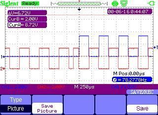
Enclosed please find the oscilloscope image of the Hi and Lo signal when I enable the Hi signal: Then due to this "stupid STM32H7 feature" the Lo signal will invert polarity, which of course is completely inacceptable for a nice power switch operation ... (this feature already destroyed one of my SLLIMM devices by effectively killing the dead time functionality...).
I think the STM32F4 did not have this feature ... no idea why the developpers sometimes seem to be so overly ambitius in creating new features when they "pimp up" older designs... . Stupid side effects sometimes then occur... .
- Labels:
-
STM32H7 series
-
TIM
- Mark as New
- Bookmark
- Subscribe
- Mute
- Subscribe to RSS Feed
- Permalink
- Email to a Friend
- Report Inappropriate Content
2020-02-05 7:21 AM
It seems to work now, if I switch the CCxNP bit together with the CCxE bit.
So I start only with the low side signal:
 pTIM->CCER= TIM_CCER_CC1NE | TIM_CCER_CC3NE |
                             TIM_CCER_CC1NP | TIM_CCER_CC3NP;
And when I startup the High side, then I take away the CCxNP bits:
pTIM->CCER= TIM_CCER_CC1E | TIM_CCER_CC3E |
                           TIM_CCER_CC1NE | TIM_CCER_CC3NE;
... so with this I can avoid that I have to switch the GPIO pin settings from AF to Output ... .
But I have to switch the CCxNP bits, so I can NOT use BDTR lock mode 2 or 3 (these would fix the polarity bits) ... of course it would NICE for such a dangerous H bridge switching to USE lock mode 2 or 3... .
- Mark as New
- Bookmark
- Subscribe
- Mute
- Subscribe to RSS Feed
- Permalink
- Email to a Friend
- Report Inappropriate Content
2020-02-05 2:46 PM
This "feature" is in the STM32 timers ever since the 'F1. I don't know the reason, my guess is that it's to increase flexibility in choice of pins for cases where the complementary output is not needed (note that the CHxN in this case copies the behaviour of if CHx would it be enabled without CHxN, i.e. it's not only the polarity but also the fact that pulse length is not influenced by deadtime).
Maybe a wee bit better solution in your case (allowing the lock) would be to swap the pins in hardware, i.e. drive the signal which needs to run from the beginning (in your case low side) from CHx, and the signal which needs to start later from CHxN.
JW
- Mark as New
- Bookmark
- Subscribe
- Mute
- Subscribe to RSS Feed
- Permalink
- Email to a Friend
- Report Inappropriate Content
2020-02-06 8:07 AM
Thank you for this input JW,
It's really good to know, that this "weird feature" has not been introduced by some "nasty STM32H7" ghost ... . If it was there already from the beginning, I am happy with it ... the STM32 timers are so nice and flexible, that I do not want to object too much ... they better in future chips should keep them as they are... .
This ingenoeusly subversive idea of using Std-Output for Lo and N-Output for Hi really works ... then I can also lock BDTR now .... just need to flip the wires on my holy PCB, but this is ok .... thank you for this.
- Mark as New
- Bookmark
- Subscribe
- Mute
- Subscribe to RSS Feed
- Permalink
- Email to a Friend
- Report Inappropriate Content
2020-02-06 8:29 AM
:D
Okay, so this was fun; now back to I2C... ;)
JW
- Timer synchronisation in STM32 MCUs Embedded software
- FreeRTOS tickless mode - ulExpectedIdleTime and HAL_SuspendTick() Problem in STM32H7 in STM32 MCUs Embedded software
- HRTIM TIMF Delayed Protection enabled despite disabled in config with LL driver on STM32G474 in STM32CubeMX (MCUs)
- SPI slave on STM32U535 in STM32 MCUs Embedded software
- FOC, Position Control used but MCM_POSITION_CONTROL of MC_ControLMode_t never used in STM32 MCUs Motor control