- STMicroelectronics Community
- STM32 MCUs
- STM32 MCUs Products
- ADC continuous conversion with DMA, last sample er...
- Subscribe to RSS Feed
- Mark Topic as New
- Mark Topic as Read
- Float this Topic for Current User
- Bookmark
- Subscribe
- Mute
- Printer Friendly Page
ADC continuous conversion with DMA, last sample error.
- Mark as New
- Bookmark
- Subscribe
- Mute
- Subscribe to RSS Feed
- Permalink
- Email to a Friend
- Report Inappropriate Content
2023-11-26 05:09 PM - edited 2023-11-26 05:58 PM
Using F401 ADC continuous conversion and DMA for multiple channels.
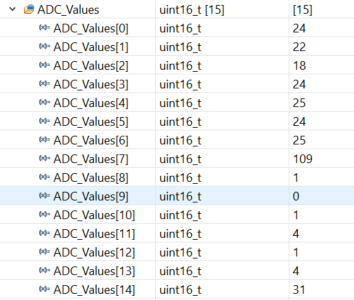
I have pins A0-7, B1, PC0-5 running conversions. For consecutive pins in a group (A0-7) (C0-5), the final pin in use always has a different offset error to the rest. Note this actually means the final /used/ pin in the group, e.g. If all 8 pins in group A are used, pinA7 has a different offset error to the rest. If only the first three 3 are used pinA2 has a different offset error to the rest. If the first 4 pins are used pinA2 no longer has the additional offset error but this is passed on to pinA3.
These results are conversions from all pins being used. The ADC inputs are grounded with pull down resistors in all cases. The different sets of values (0-4 vs18- 25) represent different input impedances from input circuits. The ADC is 12 bits so the offset errors aren't particularly problematic, the issue for me is what could be causing the last value to have a different offset error?
I've measured the pins with my oscilloscope, the B and C group are at 0 volts and the A group are approximately 20mv. I think the issue is in firmware but it's mysterious to me.
My ADC initialization code;
Solved! Go to Solution.
- Labels:
-
STM32F4 Series
Accepted Solutions
- Mark as New
- Bookmark
- Subscribe
- Mute
- Subscribe to RSS Feed
- Permalink
- Email to a Friend
- Report Inappropriate Content
2023-11-26 09:40 PM
The list of ADC Channels used didn't correspond to the pins specified. Simple mistake.
- Mark as New
- Bookmark
- Subscribe
- Mute
- Subscribe to RSS Feed
- Permalink
- Email to a Friend
- Report Inappropriate Content
2023-11-26 05:31 PM
> The ADC inputs are grounded with pull down resistors in all cases. The different sets of values (0-4 vs18- 25) represent different input impedances from input circuits.
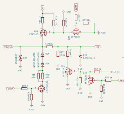
25 is a lot of counts for a grounded input. Can you show a schematic? Clearly looks like PA pins are connected differently than PB. Might help guide the answer.
- Mark as New
- Bookmark
- Subscribe
- Mute
- Subscribe to RSS Feed
- Permalink
- Email to a Friend
- Report Inappropriate Content
2023-11-26 06:09 PM
It's a multifunction input. I've removed the pull up to make sure the 20mv on the input isn't due to it. I think it's due to the resistors to ground and the leakage current of the pins, 1-3uA and 10k 1.4k 15.6k to ground.
- Mark as New
- Bookmark
- Subscribe
- Mute
- Subscribe to RSS Feed
- Permalink
- Email to a Friend
- Report Inappropriate Content
2023-11-26 09:40 PM
The list of ADC Channels used didn't correspond to the pins specified. Simple mistake.
- STM32F411 continuous DMA from ADC, how? in STM32 MCUs Embedded software
- ADC Sampling Rate for STM32G431: Practical vs Theoretical measurements in STM32 MCUs Embedded software
- How to Toggle a Debug Pin When ADC Conversion Starts in DMA Mode on STM32? in STM32 MCUs Products
- STM32H7 ADC Timer-triggered Sampling only trigger HAL_ADC_ConvCpltCallback once in STM32 MCUs Boards and hardware tools
- Code-gen problem when using file-pairs for peripheral initialization in STM32CubeMX (MCUs)

