- STMicroelectronics Community
- STM32 MCUs
- STM32 MCUs Products
- Re: Activating TIMER PWM mode with CMSIS. Need hel...
- Subscribe to RSS Feed
- Mark Topic as New
- Mark Topic as Read
- Float this Topic for Current User
- Bookmark
- Subscribe
- Mute
- Printer Friendly Page
Activating TIMER PWM mode with CMSIS. Need help!
- Mark as New
- Bookmark
- Subscribe
- Mute
- Subscribe to RSS Feed
- Permalink
- Email to a Friend
- Report Inappropriate Content
2019-11-13 12:30 AM
Hi all!
I'm fighting witn CMSIS, and now I'm triyng to start a timer in PWM mode.
The MCU is a STM32F303CCT6, and the timer I want to use is TIMER3, activating a led on PA6.
I didnt modify any clock, so I supose the MCU uses the HSI clock at 8MHz.
This is the code, but dont work. Any advice?:
/* USER CODE BEGIN 2 */

//Enable GPIOA

RCC->AHBENR |= RCC_AHBENR_GPIOAEN;

//Enable TIM3

RCC->APB1ENR |= RCC_APB1ENR_TIM3EN;

//Alternate Function 2 for A6 (TIM3 CH1)

GPIOA->AFR[0] = 0x02000000;

//Alternate mode for PA6 pin

GPIOA->MODER &= ~GPIO_MODER_MODER6_0;

GPIOA->MODER |= GPIO_MODER_MODER6_1;

//Select PWM mode 1

TIM3->CCMR1 &= ~(TIM_CCMR1_OC1M_0 | TIM_CCMR1_OC2M_3);

TIM3->CCMR1 |= TIM_CCMR1_OC1M_1 | TIM_CCMR1_OC2M_2 | TIM_CCMR1_OC1PE;

//Enabler channel 1 from TIM3

TIM3->CCER |= TIM_CCER_CC1E;

TIM3->PSC = 8000;

TIM3->ARR = 1000;

TIM3->CCR1 = 500;

TIM3->EGR |= TIM_EGR_UG;

TIM3->CR1 |= TIM_CR1_CEN;

/* USER CODE END 2 */
-
/* USER CODE BEGIN 2 */
//Enable GPIOA
RCC->AHBENR |= RCC_AHBENR_GPIOAEN;
//Enable TIM3
RCC->APB1ENR |= RCC_APB1ENR_TIM3EN;
//Alternate Function 2 for A6 (TIM3 CH1)
GPIOA->AFR[0] = 0x02000000;
//Alternate mode for PA6 pin
GPIOA->MODER &= ~GPIO_MODER_MODER6_0;
GPIOA->MODER |= GPIO_MODER_MODER6_1;
//Select PWM mode 1
TIM3->CCMR1 &= ~(TIM_CCMR1_OC1M_0 | TIM_CCMR1_OC2M_3);
TIM3->CCMR1 |= TIM_CCMR1_OC1M_1 | TIM_CCMR1_OC2M_2 | TIM_CCMR1_OC1PE;
//Enabler channel 1 from TIM3
TIM3->CCER |= TIM_CCER_CC1E;
TIM3->PSC = 8000;
TIM3->ARR = 1000;
TIM3->CCR1 = 500;
TIM3->EGR |= TIM_EGR_UG;
TIM3->CR1 |= TIM_CR1_CEN;
/* USER CODE END 2 */
Solved! Go to Solution.
- Labels:
-
STM32F3 Series
-
TIM
Accepted Solutions
- Mark as New
- Bookmark
- Subscribe
- Mute
- Subscribe to RSS Feed
- Permalink
- Email to a Friend
- Report Inappropriate Content
2019-11-13 1:58 AM
It's always good to have a look at the registers' content in the debugger, and check whether they are set as one expected.
> TIM3->CCMR1 &= ~(TIM_CCMR1_OC1M_0 | TIM_CCMR1_OC2M_3);
> TIM3->CCMR1 |= TIM_CCMR1_OC1M_1 | TIM_CCMR1_OC2M_2 | TIM_CCMR1_OC1PE;
You probably didn't intend to modify the OC2M bits.
JW
- Mark as New
- Bookmark
- Subscribe
- Mute
- Subscribe to RSS Feed
- Permalink
- Email to a Friend
- Report Inappropriate Content
2019-11-13 2:52 AM
Yes!
You're right. Thank you very much. :)
- Mark as New
- Bookmark
- Subscribe
- Mute
- Subscribe to RSS Feed
- Permalink
- Email to a Friend
- Report Inappropriate Content
2019-11-13 3:10 AM
Another question:
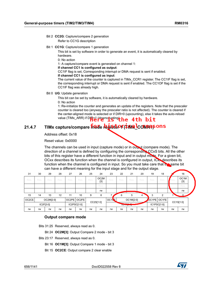
In the RM0316 file, on page 658, talk about "Bits 6:4 OC1M: Output compare 1 mode". That are 3 bits, but in the description it shows 4 bits. Whats wrong here?:
"Bits 6:4 OC1M: Output compare 1 mode
These bits define the behavior of the output reference signal OC1REF from which OC1 and
OC1N are derived. OC1REF is active high whereas OC1 and OC1N active level depends
on CC1P and CC1NP bits.
0000: Frozen - The comparison between the output compare register TIMx_CCR1 and the
counter TIMx_CNT has no effect on the outputs.(this mode is used to generate a timing
base).
0001: Set channel 1 to active level on match. OC1REF signal is forced high when the
counter TIMx_CNT matches the capture/compare register 1 (TIMx_CCR1).
..."
- Mark as New
- Bookmark
- Subscribe
- Mute
- Subscribe to RSS Feed
- Permalink
- Email to a Friend
- Report Inappropriate Content
2019-11-13 3:31 AM
JW
@Imen DAHMEN I almost certainly bragged about this in the past: can please in *all* RMs and *all* TIM chapters where this extra OC1M bit is, a footnote be added to the Bits 6:4 OC1M description, saying that OC1M[3] is to be found elsewhere?
- Mark as New
- Bookmark
- Subscribe
- Mute
- Subscribe to RSS Feed
- Permalink
- Email to a Friend
- Report Inappropriate Content
2019-11-13 3:49 AM
Thank you very much again, friend! :)
- Mark as New
- Bookmark
- Subscribe
- Mute
- Subscribe to RSS Feed
- Permalink
- Email to a Friend
- Report Inappropriate Content
2020-02-28 8:24 AM
Hi @Community member ,
I'll take care of adding the note.
For the newest versions, we have changed the description as below:
Best regards,
Vincent
- Cannot Compile When using example ioc in STM32 MCUs Wireless
- STM32F746+LWIP+CMSIS2 Not Working BUT With CMSIS1 Working in STM32 MCUs Embedded software
- Freertos v1 cmsis software timer Nucleo L476RG in STM32CubeIDE (MCUs)
- How to Properly Configure and Trigger a Soft Break on TIM1 in STM32 in STM32 MCUs Motor control
- ADC triggered by HRTimer using DMA and FreeRTOS in STM32 MCUs Embedded software

