- STMicroelectronics Community
- STM32 MCUs
- STM32 MCUs Embedded software
- Problem in SPI Interfacing of LTC1859 with STM32F4...
- Subscribe to RSS Feed
- Mark Topic as New
- Mark Topic as Read
- Float this Topic for Current User
- Bookmark
- Subscribe
- Mute
- Printer Friendly Page
Problem in SPI Interfacing of LTC1859 with STM32F401RE
- Mark as New
- Bookmark
- Subscribe
- Mute
- Subscribe to RSS Feed
- Permalink
- Email to a Friend
- Report Inappropriate Content
2018-07-06 11:45 PM
Hello,
I am using STM32F401RE microcontroller board and trying to interface LTC1859 with it. I am using STM32CUBEMX to generate code with following parameters for SPI:
Data size : 8 bits
Prescaler : 8
Clock Frequency : Changed from 84 MHz (default) to 16 MHz
First Bit : MSB first
CPOL : Low
CPHA : 2 Edge
I have configured HAL_SPI and generated the source code for ARM_V5 (keil). Following is the snippet of code used for making SPI connection between STM32 and LTC1859:
OPTION 1:
// Read Process
// 1. Pull CS or CONVST Low : ActivateHAL_GPIO_WritePin(GPIOA, GPIO_PIN_9, GPIO_PIN_RESET);// 2. Tranfer Data Read Command on MOSIspiTxBuf[1] = 0x88;//LTC1859_CH0 | LTC1859_UNIPOLAR_MODE | LTC1859_LOW_RANGE_MODE | LTC1859_NORMAL_MODE;spiTxBuf[0] = 0x00;HAL_SPI_Transmit(&hspi1, &spiTxBuf[1], 1, 50);// 3. Receive DataHAL_SPI_Receive(&hspi1, spiRxBuf, 2, 50);// 4. Pull CS or CONVST High : DeactivateHAL_GPIO_WritePin(GPIOA, GPIO_PIN_9, GPIO_PIN_SET);OPTION 2:
// Read Process
// 1. Pull CS or CONVST Low : ActivateHAL_GPIO_WritePin(GPIOA, GPIO_PIN_9, GPIO_PIN_RESET);// 2. Tranfer Data Read Command on MOSIspiTxBuf[0] = 0x88;//LTC1859_CH0 | LTC1859_UNIPOLAR_MODE | LTC1859_LOW_RANGE_MODE | LTC1859_NORMAL_MODE;spiTxBuf[1] = 0x00;HAL_SPI_TransmitReceive(&hspi1, spiTxBuf, spiRxBuf, 2, 50);// 3. Pull CS or CONVST High : DeactivateHAL_GPIO_WritePin(GPIOA, GPIO_PIN_9, GPIO_PIN_SET);Physical Connections are as follows:
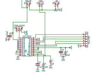
AVDD, DVDD : Connected to 5V through 10uF (tantalum) and 0.1uF (Ceramic) capacitor
OVDD : Connected to 3.3V through 1
0uF (tantalum)
COM : Connected to GND
CH0 : Input through 1000pF Ceramic capactior
SDI : SPI1_MOSI
SDO : SPI1_MISO
SCK : SPI1_SCK
CONVST & ~RD : GPIO_PIN_9
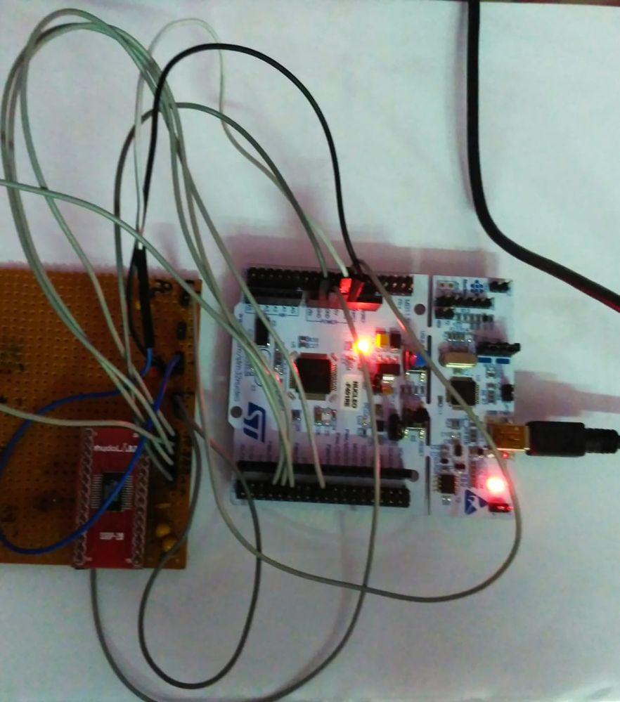
All Grounds are common.
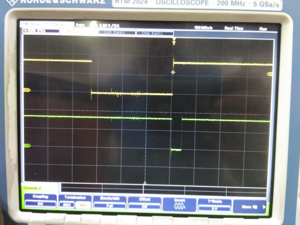
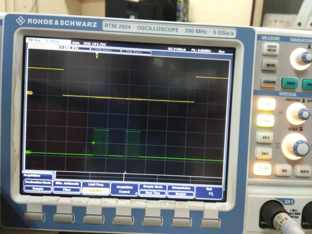
The problem I am facing is that the device is getting the communication lines in right format but not responding with ''correct'' data. Some garbage data keeps coming which is nowhere close to the data to be read. Any help would be appreciable.
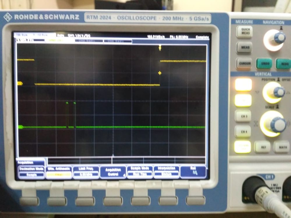
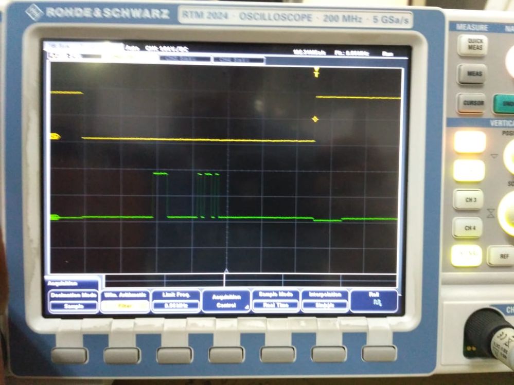
All the necessary pictures are attached herewith.
 #hal-spi #ltc1859-adc #stm32f401re-spi-keil-cubemx
- Labels:
-
STM32Cube MCU Packages
-
STM32F4 Series
- Mark as New
- Bookmark
- Subscribe
- Mute
- Subscribe to RSS Feed
- Permalink
- Email to a Friend
- Report Inappropriate Content
2018-07-07 4:12 PM
I use this style of coding :
void SPI_t::transfer(unsigned short data) {
// drop nCS// Clear_SPI1_nSS_Out();char RxSPI;
while (!(hspi1.Instance->SR & SPI_FLAG_TXE)) // wait while not empty ; *((__IO uint8_t *)&hspi1.Instance->DR) = data; // send data while (!(hspi1.Instance->SR & SPI_FLAG_TXE)) // wait while not empty ; while ((hspi1.Instance->SR & SPI_FLAG_BSY)) // wait while still transferring to pin ; while ((hspi1.Instance->SR & SPI_FLAG_RXNE)) //take all bytes in the receiver, we only want the last one. RxSPI = hspi1.Instance->DR; // Set_SPI1_nSS_Out(); }- Mark as New
- Bookmark
- Subscribe
- Mute
- Subscribe to RSS Feed
- Permalink
- Email to a Friend
- Report Inappropriate Content
2018-07-08 1:08 AM
Thanks for reply.
As I see, set and reset of nSS pin would mean to simple HAL_GPIO_WritePin to CONVST (for this particular ADC).
Next the ADC responds with 2 bytes of data in the current communication cycle:
1. While transmitting 1 byte on MOSI, first byte is received on MISO.
2. Next byte is received in next set of 8-bit SCLK of the same communication cycle.
In the snippet you provided, first it is waiting for Tx to complete on MOSI and then read the data of MISO. How to make it a duplex transmission/reception? (by removing
while ((hspi1.Instance->SR & SPI_FLAG_BSY)) ??)As in my code I was using HAL_SPI_TransmitReceive() send and receive at the same time on a particular communication cycle.
For 2 byte reception shall I make RxSPI a uint16_t type of variable?
- Mark as New
- Bookmark
- Subscribe
- Mute
- Subscribe to RSS Feed
- Permalink
- Email to a Friend
- Report Inappropriate Content
2018-07-08 2:25 AM
I tried running your function:
uint8_t SPI_tx(uint8_t txdata) {
// drop nCS
// Clear_SPI1_nSS_Out();
// 1. Pull CS or CONVST Low : Activate
HAL_GPIO_WritePin(GPIOA, GPIO_PIN_9, GPIO_PIN_RESET);
uint8_t RxSPI;
while (!(hspi1.Instance->SR & SPI_FLAG_TXE)) // wait while not empty
;
*((__IO uint8_t *)&hspi1.Instance->DR) = txdata; // send data
while (!(hspi1.Instance->SR & SPI_FLAG_TXE)) // wait while not empty
;
while ((hspi1.Instance->SR & SPI_FLAG_BSY)) // wait while still transferring to pin
;
while ((hspi1.Instance->SR & SPI_FLAG_RXNE)) //take all bytes in the receiver, we only want the last one.
RxSPI = hspi1.Instance->DR;
// 1. Pull CS or CONVST High : Deactivate
HAL_GPIO_WritePin(GPIOA, GPIO_PIN_9, GPIO_PIN_SET);
// Set_SPI1_nSS_Out();
return RxSPI;
}
�?�?�?�?�?�?�?�?�?�?�?�?�?�?�?�?�?�?�?�?�?�?�?�?
I do not have scope right now but when I put it into debug mode, I can see that the control is stuck at
while (!(hspi1.Instance->SR & SPI_FLAG_TXE));�?and nothing is received in the Rx buffer at all. However in my original code, as you may see from the scope, Tx buffer is correctly writing 1 byte of required data, while Rx buffer is also receiving something in 2 SCLK in a communication cycle of SPI. That's how it should be. But my problem is that, the data read on Rx line is not meaningful corresponding to Input I give. Whether I give
1. 0V (GND) Rx buffer keeps fluctuating
2. or 3V, Rx buffer is still fluctuating giving an output value that in no way matches the given input.
Please help.
- Mark as New
- Bookmark
- Subscribe
- Mute
- Subscribe to RSS Feed
- Permalink
- Email to a Friend
- Report Inappropriate Content
2018-07-08 6:40 PM
When you can get to a scope, please check your nSS functionality is working, I had some trouble...:(
void Set_SPI1_nSS_Out(void) {
SPI1_nSS_Out_GPIO_Port->ODR |= SPI1_nSS_Out_Pin; // pin up}void Clear_SPI1_nSS_Out(void) {
SPI1_nSS_Out_GPIO_Port->ODR &= ~SPI1_nSS_Out_Pin; // pin down}- stm32f401re X-NUCLEO-BNRG2A1 interface with ISM330DHCX in STM32 MCUs Products
- The interface firmware FAILED to reset/halt the target MCU with STM32F401RE in STM32 MCUs Boards and hardware tools
- how to interface LoRa 993 with stm32f401RE in STM32CubeIDE (MCUs)
- How to use DMD P10 LED displays with STM32 in STM32 MCUs Products
- Hello! I am trying to interface IC max7219 (Serial interfaced led driver) with STM32F401RE through SPI communication.I am finding irregular functionality in logic analyser.Please help in STM32 MCUs Products