- STMicroelectronics Community
- STM32 MCUs
- STM32 MCUs Embedded software
- Re: F767ZI issue using IAP with Dual Bank Flash
- Subscribe to RSS Feed
- Mark Topic as New
- Mark Topic as Read
- Float this Topic for Current User
- Bookmark
- Subscribe
- Mute
- Printer Friendly Page
F767ZI issue using IAP with Dual Bank Flash
- Mark as New
- Bookmark
- Subscribe
- Mute
- Subscribe to RSS Feed
- Permalink
- Email to a Friend
- Report Inappropriate Content
2018-02-09 3:46 PM
Im Using STM32F767ZI Nucleo Board which has 2Mbytes of flash for code storage. It also allows for the flash to be evenly divided between two banks. This gives bank 1 one Mbyte of data, and bank 2 one Mbyte of data.
Bank 1 Address offset in Flash is0x08000000
Bank 2 Address offset in Flash is0x08100000
With the use of nDBOOT = nDBANK = 0 option bytes the memory is configured in the dual bank, dual boot mode.
My Current Testing Procedure:
Step 1) I compile the firmwarewhich has a single byte indicating the version of the firmware. I compile it twice once with version byte as 1, and once with version byte as 2. Otherwise its identical code.
Step 2) I use STM32 ST-Link Utility to manually program each version into each bank and run it. I do this for both version with both banks, so 4 times.
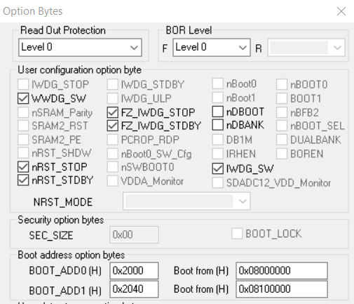
I use the following option bytes to run from bank 1 while programming the .bin at offset for Bank 1:

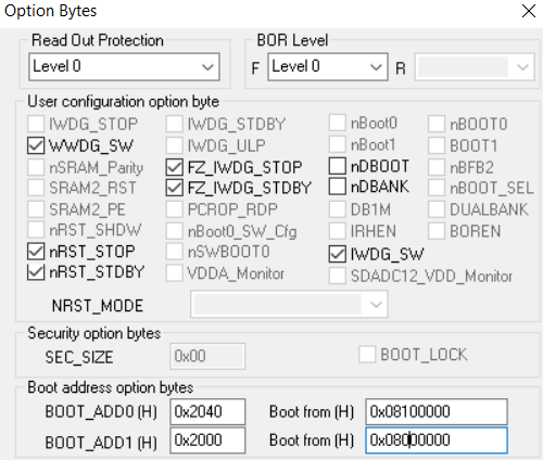
And i use the following option bytes to run from bank 2 while programming the .bin at offset for Bank 2:
All of this up to this point works as expected and im able to read out the different versions from each of the banks.
Step 3) I load version 1 into bank 1 using method above and i use the following code to programmatically erase/program bank 2 with Version 2 firmware.
HAL_FLASH_Unlock(); /* Unlock the Flash to enable the flash control register access *************/
HAL_FLASH_OB_Unlock(); /* Allow Access to option bytes sector */
FLASH_EraseInitTypeDef pEraseInit;
if ((SYSCFG->MEMRMP & SYSCFG_MEMRMP_SWP_FB) == RESET) //Test if Bank == 1
{
 pEraseInit.Banks = FLASH_BANK_2;
 pEraseInit.TypeErase = FLASH_TYPEERASE_MASSERASE;
 pEraseInit.VoltageRange = VOLTAGE_RANGE_3;
 uint32_t SectorError = 0;
 halstatus = HAL_FLASHEx_Erase(&pEraseInit, &SectorError);
 if(halstatus != HAL_OK)
 {
 return 15;
 }
}
else
{
 pEraseInit.Banks = FLASH_BANK_1;
 pEraseInit.TypeErase = FLASH_TYPEERASE_MASSERASE;
 pEraseInit.VoltageRange = VOLTAGE_RANGE_3;
 uint32_t SectorError = 0;
 halstatus = HAL_FLASHEx_Erase(&pEraseInit, &SectorError);
 if(halstatus != HAL_OK)
 {
 return 15;
 }
}�?�?�?�?�?�?�?�?�?�?�?�?�?�?�?�?�?�?�?�?�?�?�?�?�?�?�?�?�?�?�?�?�?�?�?�?�?�?�?�?�?�?�?�?�?�?�?�?�?�?�?�?�?�?
And use this code to actually program it
uint32_t BaseAddress = 0;
if ((SYSCFG->MEMRMP & SYSCFG_MEMRMP_SWP_FB) == RESET) //Test if Bank == 1
{
 BaseAddress = 0x08100000;
}
else
{
 BaseAddress = 0x08000000;
}
HAL_FLASH_Unlock();
HAL_FLASH_OB_Unlock();
__HAL_FLASH_CLEAR_FLAG(FLASH_FLAG_WRPERR);
__HAL_FLASH_CLEAR_FLAG(FLASH_FLAG_ALL_ERRORS);
for(int i = 0; i < 48; i++)
{
 halstatus = HAL_FLASH_Program(FLASH_TYPEPROGRAM_BYTE,BaseAddress + FirmwareAddressOffset + i,FirmwareData[i]);
 if(halstatus != HAL_OK)
 {
 return 4; //Error 4
 }
}
int verified = 0;
uint8_t val = 0;
for(int i = 0; i < 48; i++)
{
 val = *(__IO uint8_t *) (BaseAddress + FirmwareAddressOffset + i);
 if(val == FirmwareData[i])
 {
 verified++;
 }
 //verified++; //Added for Debug
}
if(verified == 48)
{
 FirmwareAddressOffset = FirmwareAddressOffset + 48;
 return 3;//OK
}
else
{
 return 4;//Error
}�?�?�?�?�?�?�?�?�?�?�?�?�?�?�?�?�?�?�?�?�?�?�?�?�?�?�?�?�?�?�?�?�?�?�?�?�?�?�?�?�?�?�?�?�?�?�?�?�?�?�?�?�?�?�?�?�?�?�?�?�?�?�?�?�?�?�?�?�?�?�?�?�?�?�?�?�?�?�?�?�?�?
Once its all done i use the following code to actually switch the banks
HAL_FLASH_OB_Unlock();
FLASH_OBProgramInitTypeDef flashConfig;
if ((SYSCFG->MEMRMP & SYSCFG_MEMRMP_SWP_FB) == RESET) //Test if Bank == 1
{
 //Switch boot to bank 2, should be done at the end of update
 FLASH_WaitForLastOperation(9000);
 HAL_FLASHEx_OBGetConfig(&flashConfig);
 flashConfig.BootAddr0 = 0x2040;
 flashConfig.BootAddr1 = 0x2000;
 HAL_FLASHEx_OBProgram(&flashConfig);
}
else
{
 //Switch boot to bank 1, should be done at the end of update
 FLASH_WaitForLastOperation(9000);
 HAL_FLASHEx_OBGetConfig(&flashConfig);
 flashConfig.BootAddr0 = 0x2000;
 flashConfig.BootAddr1 = 0x2040;
 HAL_FLASHEx_OBProgram(&flashConfig);
}
HAL_FLASH_OB_Launch();
NVIC_SystemReset();�?�?�?�?�?�?�?�?�?�?�?�?�?�?�?�?�?�?�?�?�?�?�?�?�?�?�?�?�?�?�?�?�?�?�?�?�?�?�?�?�?�?�?�?�?�?�?�?�?�?�?�?�?�?�?�?�?�?�?�?�?�?�?�?�?�?�?�?
So for Step 3 This works. It loads version 2 into Bank 2 and starts running it. I can see version 2 being output, and after i hit hard reset it again loads the new firmware from Bank 2. All is as expected here.
My problem is as follows:
When i try to program version 1 or version 2 into Bank 2 and run the upgrade process it never is able to program anything into bank 1. It can erase it but the actual program never happens even though no errors are reported except when it actually tries to verify the memory against the live data. When i look at the Bank 1 memory after programming from Bank 2 its all 0xFFFF.
I need help to figure out whyit is able to program Bank 2 from Bank 1, but fails to program Bank 1 when running from Bank 2?
-Andriy
#dual-bank #flash #dual-boot #stm32 #hal #iap #firmware-update #f7Solved! Go to Solution.
Accepted Solutions
- Mark as New
- Bookmark
- Subscribe
- Mute
- Subscribe to RSS Feed
- Permalink
- Email to a Friend
- Report Inappropriate Content
2018-02-12 5:27 AM
When programming, always program to the Bank2 address since the executing bank is always remapped to the Bank1 address.
- Mark as New
- Bookmark
- Subscribe
- Mute
- Subscribe to RSS Feed
- Permalink
- Email to a Friend
- Report Inappropriate Content
2018-02-12 5:27 AM
When programming, always program to the Bank2 address since the executing bank is always remapped to the Bank1 address.
- Mark as New
- Bookmark
- Subscribe
- Mute
- Subscribe to RSS Feed
- Permalink
- Email to a Friend
- Report Inappropriate Content
2018-02-12 10:03 AM
Yes that was my issue. Thanks for your help.
- Mark as New
- Bookmark
- Subscribe
- Mute
- Subscribe to RSS Feed
- Permalink
- Email to a Friend
- Report Inappropriate Content
2018-02-21 1:03 PM
Hi Yarema,
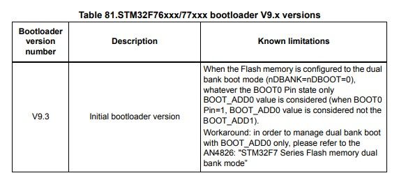
Just be aware that BOOT_ADD1 won't work when you have
nDBOOT = nDBANK = 0There is a Known limitation of the bootloader for this processor. It is in AN2606 document.

They just updated this document this month and it is there still.
- Mark as New
- Bookmark
- Subscribe
- Mute
- Subscribe to RSS Feed
- Permalink
- Email to a Friend
- Report Inappropriate Content
2018-02-21 7:13 PM
HAL_FLASH_OB_Unlock();
FLASH_OBProgramInitTypeDef flashConfig;
if ((SYSCFG->MEMRMP & SYSCFG_MEMRMP_SWP_FB) == RESET) //Test if Bank == 1
{
 //Switch boot to bank 2, should be done at the end of update
 FLASH_WaitForLastOperation(9000);
 HAL_FLASHEx_OBGetConfig(&flashConfig);
 flashConfig.BootAddr0 = 0x2040;
 flashConfig.BootAddr1 = 0x2000;
 HAL_FLASHEx_OBProgram(&flashConfig);
}
else
{
 //Switch boot to bank 1, should be done at the end of update
 FLASH_WaitForLastOperation(9000);
 HAL_FLASHEx_OBGetConfig(&flashConfig);
 flashConfig.BootAddr0 = 0x2000;
 flashConfig.BootAddr1 = 0x2040;
 HAL_FLASHEx_OBProgram(&flashConfig);
}
HAL_FLASH_OB_Launch();
NVIC_SystemReset();
Above is how i currently swap banks, notice the addresses written for BootAddr0. So as it happens, the behavior you are describing is the exact behavior i want since this is meant to serve as storage for a complete firmware set in one of the banks, and a 'dont care' in the other bank.
My goal with this is to be able to update firmware in the field by writing the new firmware into the bank that its currently not using, and restarting the system with execution now only from that other bank.
-Andriy
- Mark as New
- Bookmark
- Subscribe
- Mute
- Subscribe to RSS Feed
- Permalink
- Email to a Friend
- Report Inappropriate Content
2018-10-21 9:11 AM
Hi Yarema,
- Mark as New
- Bookmark
- Subscribe
- Mute
- Subscribe to RSS Feed
- Permalink
- Email to a Friend
- Report Inappropriate Content
2018-10-21 9:18 AM
Hi Yarema,
I'm facing exactly same issue like you. With your example code, I can reproduce the issue just like my own application.
The weird part is even I changed the source to always program to the Bank2 address, nothing improved. Bank 1 memory after programming from Bank 2 its all 0xFFFF.
Could you share your details to fix this issue? any information will be appreciated!
-Jun
- Mark as New
- Bookmark
- Subscribe
- Mute
- Subscribe to RSS Feed
- Permalink
- Email to a Friend
- Report Inappropriate Content
2018-10-21 11:02 AM
As far as code the above is what i still use with this section changed to be the following:
if ((SYSCFG->MEMRMP & SYSCFG_MEMRMP_SWP_FB) == RESET) //Test if Bank == 1
{
 BaseAddress = 0x08100000;
}
else
{
 BaseAddress = 0x08100000;
}
To actually get it to work you need to use STM32CubeProgrammer to program the options bytes such that NBOOT = NBANK = 0 (unchecked), otherwise it operates in single bank mode.
- Mark as New
- Bookmark
- Subscribe
- Mute
- Subscribe to RSS Feed
- Permalink
- Email to a Friend
- Report Inappropriate Content
2018-10-21 2:13 PM
Hi Yarema,
Thanks for the prompt response. I changed related source same like you, and NBOOT=NBANK=0 was unchecked by ST-Link Utility. STM32CubeProgrammer was tried too, but same issue existed.
Below are my current source, Same firmware was copied from 0x08000000 to FirmwareData array, and be updated to 0x08000000. I set the value of "FirmwareAddressOffset" to 0.
uint8_t FirmwareData[8*16*16*16];
uint32_t FirmwareAddressOffset = 0;

uint16_t ProgramFlash( uint32_t FirmwareDataLength )
{
  uint32_t BaseAddress = 0;

  memcpy( (uint8_t*)FirmwareData, (uint8_t*)0x08000000U, FirmwareDataLength );
  if ((SYSCFG->MEMRMP & SYSCFG_MEMRMP_SWP_FB) == RESET) //Test if Bank == 1
  {
    BaseAddress = 0x08100000U;
  }
  else
  {
    BaseAddress = 0x08100000U;
  }

  HAL_FLASH_Unlock();
  HAL_FLASH_OB_Unlock();
  __HAL_FLASH_CLEAR_FLAG(FLASH_FLAG_WRPERR);
  __HAL_FLASH_CLEAR_FLAG(FLASH_FLAG_ALL_ERRORS);
  for(int i = 0; i < FirmwareDataLength; i++)
  {
    halstatus = HAL_FLASH_Program( FLASH_TYPEPROGRAM_BYTE, BaseAddress + FirmwareAddressOffset + i,FirmwareData[i]);
    if(halstatus != HAL_OK)
    {
      return 4; //Error 4
    }
  }
  int verified = 0;
  uint8_t val = 0;
  for(int i = 0; i < 48; i++)
  {
    val = *(__IO uint8_t *) (BaseAddress + FirmwareAddressOffset + i);
    if(val == FirmwareData[i])
    {
      verified++;
    }
    //verified++; //Added for Debug
  }
  if(verified == FirmwareDataLength)
  {
    FirmwareAddressOffset = FirmwareAddressOffset + FirmwareDataLength;
    return 3;//OK
  }
  else
  {
    return 4;//Error
  }
}

void SwitchBank( void )
{
  HAL_FLASH_OB_Unlock();
  FLASH_OBProgramInitTypeDef flashConfig;
  if ((SYSCFG->MEMRMP & SYSCFG_MEMRMP_SWP_FB) == RESET) //Test if Bank == 1
  {
    //Switch boot to bank 2, should be done at the end of update
    FLASH_WaitForLastOperation(90000);
    HAL_FLASHEx_OBGetConfig(&flashConfig);
    flashConfig.BootAddr0 = 0x2040;
    flashConfig.BootAddr1 = 0x2000;
    HAL_FLASHEx_OBProgram(&flashConfig);
  }
  else
  {
    //Switch boot to bank 1, should be done at the end of update
    FLASH_WaitForLastOperation(90000);
    HAL_FLASHEx_OBGetConfig(&flashConfig);
    flashConfig.BootAddr0 = 0x2000;
    flashConfig.BootAddr1 = 0x2040;
    HAL_FLASHEx_OBProgram(&flashConfig);
  }
  HAL_FLASH_OB_Launch();
  NVIC_SystemReset();
}
In main function I called this functions in this way. If user button was pushed, firmware update will be started.
  while (1)
  {
    /* Wait for BUTTON_USER is released */
    if (BSP_PB_GetState(BUTTON_USER) == SET)
    {
      while (BSP_PB_GetState(BUTTON_USER) == SET);
      EraseSector();
      ProgramFlash( hBufferSize );
      SwitchBank();
   }
   else
    {
      if ( (SYSCFG->MEMRMP & SYSCFG_MEMRMP_SWP_FB) == RESET ){
        BSP_LED_Toggle(LED1);
      }
      else {
        BSP_LED_Toggle(LED2);
      }
      /* Insert 200 ms delay */
      HAL_Delay(200);
    }
}
I'm using STM32F769I-Discovery to test these source code, is it same as your platform?
could you help to see if there's anything wrong with my code, Thanks!
- Mark as New
- Bookmark
- Subscribe
- Mute
- Subscribe to RSS Feed
- Permalink
- Email to a Friend
- Report Inappropriate Content
2018-10-21 2:21 PM
In my case im using F767ZI Nucleo. Have you tried just programming test data into bank 2 while running from Bank 1 to see if you are able to then read it with the STM32CubeProgrammer tool?
Also not sure what your EraseSector() function does but i erase the other bank with the following code.
HAL_FLASH_Unlock(); /* Unlock the Flash to enable the flash control register access *************/
HAL_FLASH_OB_Unlock(); /* Allow Access to option bytes sector */
FLASH_EraseInitTypeDef pEraseInit;
if ((SYSCFG->MEMRMP & SYSCFG_MEMRMP_SWP_FB) == RESET) //Test if Bank == 1
{
	pEraseInit.Banks = FLASH_BANK_2;
	pEraseInit.TypeErase = FLASH_TYPEERASE_MASSERASE;
	pEraseInit.VoltageRange  = VOLTAGE_RANGE_3;
	uint32_t SectorError = 0;
	halstatus = HAL_FLASHEx_Erase(&pEraseInit, &SectorError);
	if(halstatus != HAL_OK)
	{
		return 15;
	}
}
else
{
	pEraseInit.Banks = FLASH_BANK_1;
	pEraseInit.TypeErase = FLASH_TYPEERASE_MASSERASE;
	pEraseInit.VoltageRange  = VOLTAGE_RANGE_3;
	uint32_t SectorError = 0;
	halstatus = HAL_FLASHEx_Erase(&pEraseInit, &SectorError);
	if(halstatus != HAL_OK)
	{
		return 15;
	}
}- I want to transmit adc values to hercules while using ibus protocol. in STM32 MCUs Embedded software
- Double ECC Error inject for STM32L5/U5 in STM32 MCUs Products
- STM32U5 - ICACHE with XIP from OCTOSPI - Breakpoints and General Setup in STM32 MCUs Products
- STM32WB FLASH write/erase issue after reset in STM32 MCUs Wireless
- Bricked two STM32WBA55 NUCLEO boards by flashing in CubeIDE (repeteable) in STM32 MCUs Products
