- STMicroelectronics Community
- STM32 MCUs
- STM32 MCUs Embedded software
- Re: DMA PWM outputs 2 pulses per buffer value (STM...
- Subscribe to RSS Feed
- Mark Topic as New
- Mark Topic as Read
- Float this Topic for Current User
- Bookmark
- Subscribe
- Mute
- Printer Friendly Page
DMA PWM outputs 2 pulses per buffer value (STM32l072xx)
- Mark as New
- Bookmark
- Subscribe
- Mute
- Subscribe to RSS Feed
- Permalink
- Email to a Friend
- Report Inappropriate Content
2019-09-28 12:04 AM
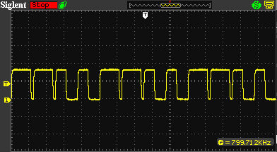
I'm trying to use DMA in circular mode to modify the duty cycle of a PWM output. Ultimately, I plan to use it to communicate with WS2812B chips (like others have done with the STM32F4 chips). However, in my early tests I've noticed that it seems to send two pulses per buffer value.
For a simple example (full code at the end):
#define BUFFER_SIZE 2

uint16_t buffer[BUFFER_SIZE];
buffer[0] = htim3.Init.Period * .5; // 50%
buffer[1] = htim3.Init.Period * .9; // 90%

HAL_TIM_PWM_Start_DMA(&htim3, TIM_CHANNEL_1, (uint32_t*)buffer, BUFFER_SIZE);
There are 2 items in the buffer, one set at 50% duty cycle and the other at 90%. When circular mode is enabled, I would expect to see the PWM pulse to be alternating between the two. However, I see 2 pulses at 50% followed by 2 at 90%, and so on.
I'm sure I'm missing something elementary here. How do I get the pulses to alternate 50%, 90%, 50%, etc?
One of my thoughts was that the duplication could be caused by data width conversion on the data bus, as explained in section 11.3.4, page 268, of the reference manual (i.e. 16-bit value on a 32-bit bus) However, changing the DMA Data Alignment values doesn't change this.
Any ideas? Here's the code, which is based on the boiler plate created by STM32Cube:
#include <stdint.h>
#include "main.h"

#define SIGNAL_HZ 800000 // 800kHz
#define BUFFER_SIZE 2

TIM_HandleTypeDef htim3;
DMA_HandleTypeDef hdma_tim3_ch1;
uint16_t buffer[BUFFER_SIZE];

void SystemClock_Config(void);
static void MX_GPIO_Init(void);
static void MX_TIM3_Init(void);
static void MX_DMA_Init(void);

/**
  * @brief  The application entry point.
  * @retval int
  */
int main(void) {
  HAL_Init();
  SystemClock_Config();
  MX_GPIO_Init();
  MX_DMA_Init();
  MX_TIM3_Init();

  // PWM Buffer
  buffer[0] = htim3.Init.Period * .5; // 50%
  buffer[1] = htim3.Init.Period * .9; // 90%

  // Start DMA -> PWM
  HAL_TIM_PWM_Start_DMA(&htim3, TIM_CHANNEL_1, (uint32_t*)buffer, BUFFER_SIZE);

  while (1) { }
}

/**
  * @brief System Clock Configuration
  * @retval None
  */
void SystemClock_Config(void)
{
  RCC_OscInitTypeDef RCC_OscInitStruct = {0};
  RCC_ClkInitTypeDef RCC_ClkInitStruct = {0};

  __HAL_PWR_VOLTAGESCALING_CONFIG(PWR_REGULATOR_VOLTAGE_SCALE1);

  // Oscillator init config
  RCC_OscInitStruct.OscillatorType = RCC_OSCILLATORTYPE_HSI;
  RCC_OscInitStruct.HSIState = RCC_HSI_ON;
  RCC_OscInitStruct.HSICalibrationValue = RCC_HSICALIBRATION_DEFAULT;
  RCC_OscInitStruct.PLL.PLLState = RCC_PLL_ON;
  RCC_OscInitStruct.PLL.PLLSource = RCC_PLLSOURCE_HSI;
  RCC_OscInitStruct.PLL.PLLMUL = RCC_PLLMUL_4;
  RCC_OscInitStruct.PLL.PLLDIV = RCC_PLLDIV_2;
  if (HAL_RCC_OscConfig(&RCC_OscInitStruct) != HAL_OK) {
    Error_Handler();
  }

  // Clock init config
  RCC_ClkInitStruct.ClockType = RCC_CLOCKTYPE_HCLK|RCC_CLOCKTYPE_SYSCLK
                              |RCC_CLOCKTYPE_PCLK1|RCC_CLOCKTYPE_PCLK2;
  RCC_ClkInitStruct.SYSCLKSource = RCC_SYSCLKSOURCE_PLLCLK;
  RCC_ClkInitStruct.AHBCLKDivider = RCC_SYSCLK_DIV1;
  RCC_ClkInitStruct.APB1CLKDivider = RCC_HCLK_DIV1;
  RCC_ClkInitStruct.APB2CLKDivider = RCC_HCLK_DIV1;
  if (HAL_RCC_ClockConfig(&RCC_ClkInitStruct, FLASH_LATENCY_1) != HAL_OK) {
    Error_Handler();
  }
}

/**
  * @brief TIM3 Initialization Function
  * @param None
  * @retval None
  */
static void MX_TIM3_Init(void) {
  TIM_MasterConfigTypeDef sMasterConfig = {0};
  TIM_OC_InitTypeDef sConfigOC = {0};

  __HAL_RCC_TIM3_CLK_ENABLE();

  htim3.Instance = TIM3;
  htim3.Init.Prescaler = 0;
  htim3.Init.CounterMode = TIM_COUNTERMODE_UP;
  htim3.Init.Period = (SystemCoreClock / SIGNAL_HZ) - 1;
  htim3.Init.ClockDivision = TIM_CLOCKDIVISION_DIV1;
  htim3.Init.AutoReloadPreload = TIM_AUTORELOAD_PRELOAD_ENABLE;
  if (HAL_TIM_PWM_Init(&htim3) != HAL_OK) {
    Error_Handler();
  }

  sMasterConfig.MasterOutputTrigger = TIM_TRGO_RESET;
  sMasterConfig.MasterSlaveMode = TIM_MASTERSLAVEMODE_DISABLE;
  if (HAL_TIMEx_MasterConfigSynchronization(&htim3, &sMasterConfig) != HAL_OK) {
    Error_Handler();
  }

  sConfigOC.OCMode = TIM_OCMODE_PWM1;
  sConfigOC.Pulse = 0;
  sConfigOC.OCPolarity = TIM_OCPOLARITY_HIGH;
  sConfigOC.OCFastMode = TIM_OCFAST_ENABLE;
  if (HAL_TIM_PWM_ConfigChannel(&htim3, &sConfigOC, TIM_CHANNEL_1) != HAL_OK) {
    Error_Handler();
  }
  if (HAL_TIMEx_RemapConfig(&htim3, TIM3_TI1_GPIO) != HAL_OK) {
    Error_Handler();
  }
}

/**
  * Enable DMA controller clock
  */
static void MX_DMA_Init(void){
  __HAL_RCC_DMA1_CLK_ENABLE();

  hdma_tim3_ch1.Instance = DMA1_Channel5;
  hdma_tim3_ch1.Init.Request = DMA_REQUEST_10;
  hdma_tim3_ch1.Init.Direction = DMA_MEMORY_TO_PERIPH;
  hdma_tim3_ch1.Init.PeriphInc = DMA_PINC_DISABLE;
  hdma_tim3_ch1.Init.MemInc = DMA_MINC_ENABLE;
  hdma_tim3_ch1.Init.PeriphDataAlignment = DMA_PDATAALIGN_WORD; // 16-bit PWM, but 32-bit bus
  hdma_tim3_ch1.Init.MemDataAlignment = DMA_MDATAALIGN_HALFWORD;
  hdma_tim3_ch1.Init.Mode = DMA_CIRCULAR;
  hdma_tim3_ch1.Init.Priority = DMA_PRIORITY_LOW;
  if (HAL_DMA_Init(&hdma_tim3_ch1) != HAL_OK) {
    Error_Handler();
  }
  __HAL_LINKDMA(&htim3, hdma[TIM_DMA_ID_CC1], hdma_tim3_ch1);
}

/**
  * @brief GPIO Initialization Function
  * @param None
  * @retval None
  */
static void MX_GPIO_Init(void) {
  GPIO_InitTypeDef GPIO_PWMStruct = {0};
  __HAL_RCC_GPIOA_CLK_ENABLE();

  // PWM output pin - PA6
  GPIO_PWMStruct.Pin = GPIO_PIN_6;
  GPIO_PWMStruct.Mode = GPIO_MODE_AF_PP;
  GPIO_PWMStruct.Pull = GPIO_PULLDOWN;
  GPIO_PWMStruct.Speed = GPIO_SPEED_FREQ_VERY_HIGH;
  GPIO_PWMStruct.Alternate = GPIO_AF2_TIM3;
  HAL_GPIO_Init(GPIOA, &GPIO_PWMStruct);
}

/**
  * @brief  This function is executed in case of error occurrence.
  * @retval None
  */
void Error_Handler(void) {
}
Solved! Go to Solution.
- Labels:
-
DMA
-
STM32Cube MCU Packages
-
STM32L0 Series
-
TIM
Accepted Solutions
- Mark as New
- Bookmark
- Subscribe
- Mute
- Subscribe to RSS Feed
- Permalink
- Email to a Friend
- Report Inappropriate Content
2019-09-30 12:43 PM
The problem is a combination of
- CCRx being preloaded, i.e. value written to CCRx gets "active" (in ST lingo, gets copied into the shadow register, where the shadow is the "acting" register, not directly visible to the programmer but governing the behaviour) only after the next Update event (that's when CNT==ARR and then rolls over to zero) - this is witnessed by TIMx_CCMR1.OC1PE = 1 (btw. OC1FE is irrelevant here; it's a marginal feature only when the timer is triggered from some other signal, this is not the case)
- DMA is driven from CC event (TIMx_DIER.CC1DE = 1)
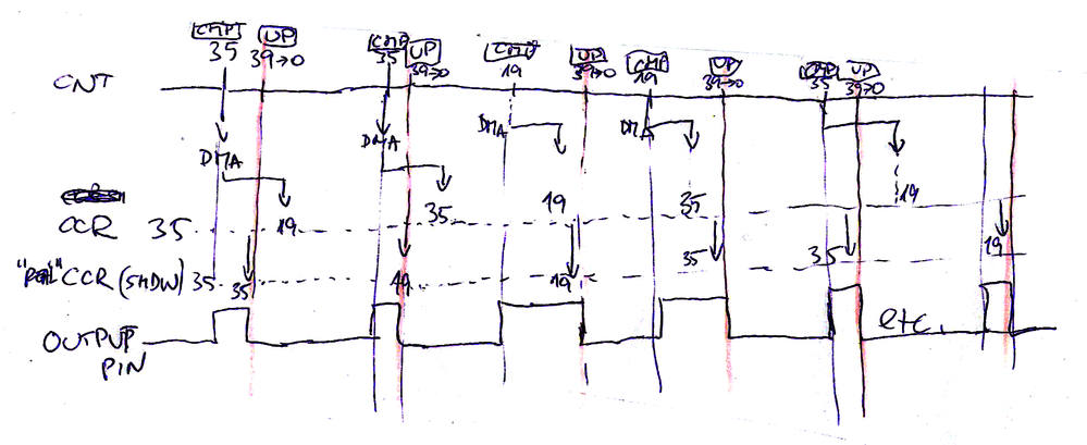
- timing is too tight, i.e. with the CC set to 90%, at the time when DMA finishes the nest Update has already passed - DMA takes maybe a dozen cycles depending on several different circumstances, from the trigger to writing to the target - here, at the 90% there are only 4 cycles, that's too few - read AN2548 for the painful details
I've made this back of the envelope drawing, but these things tend to get much clearer if *you* make this or similar drawing:
The remedy is simple, don't trigger DMA from CC, but from Update, i.e. don't set TIMx_DIER.CC1DE, but TIMx_DIER.UDE.
It maybe will then also be a different channel in DMA and different setting in its triggers-inputs-mux, look it up in the DMA chapter).
I don't Cube.
JW
- Mark as New
- Bookmark
- Subscribe
- Mute
- Subscribe to RSS Feed
- Permalink
- Email to a Friend
- Report Inappropriate Content
2019-09-28 2:46 AM
I am honestly puzzled.
Read out and post the content of relevant DMA and TIM registers.
JW
- Mark as New
- Bookmark
- Subscribe
- Mute
- Subscribe to RSS Feed
- Permalink
- Email to a Friend
- Report Inappropriate Content
2019-09-30 9:54 AM
Some register values and a few more thoughts/questions:
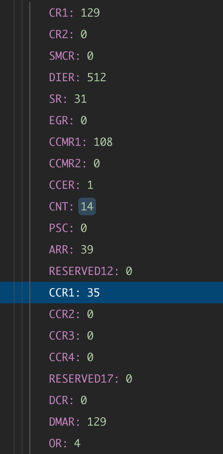
Some of the TIM3 registers, using GDB:
I paused the application several times and can confirm the correct number is being set to CCR1. I cannot track the the value in real-time, since it's being transferred outside of CPU operations.
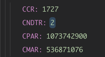
I'm not sure which DMA registers would help us here, but here are some of them:
I'm new to DMA, so I'd love to check my assumptions from what I've read about how this should work...
When setting DMA to memory -> peripheral (TIM). As I understand it, the peripheral (TIM3, in this case) will make a request to the DMA controller to receive the next value from memory. DMA will then send the value and, in this case, increment the memory location pointer for the next request.
Assumptions/Questions:
- Assumption 1: The request comes from the timer? (assumption from section 11.3.1 of the reference manual)
- Assumption 2: The request is made with the output compare event. (from section 20.2 of the reference manual)
- Q 2.1: Could the issue be with the event the timer uses to make a request to the DMA controller? What could affect this?
It almost seems like a timer repetition counter is set to 2, but from what I can tell the STM32l0xx doesn't have a repetition counter.
The next thing I'm going to try is using the transfer complete flag in the DMA interrupt to toggle an output pin and see how that lines up with the other signal on the scope. That won't tell me a lot, but it might give me another piece of information.
- Mark as New
- Bookmark
- Subscribe
- Mute
- Subscribe to RSS Feed
- Permalink
- Email to a Friend
- Report Inappropriate Content
2019-09-30 12:42 PM
Another thought. Looking at the timer registers, DIER has UDE (bit 8 - Update DMA request enable) set to 0. This could be affecting the request event, even though tthe CC1DE (bit 9 - Capture/Compare 1 DMA request enable) is enabled.
- Mark as New
- Bookmark
- Subscribe
- Mute
- Subscribe to RSS Feed
- Permalink
- Email to a Friend
- Report Inappropriate Content
2019-09-30 12:43 PM
The problem is a combination of
- CCRx being preloaded, i.e. value written to CCRx gets "active" (in ST lingo, gets copied into the shadow register, where the shadow is the "acting" register, not directly visible to the programmer but governing the behaviour) only after the next Update event (that's when CNT==ARR and then rolls over to zero) - this is witnessed by TIMx_CCMR1.OC1PE = 1 (btw. OC1FE is irrelevant here; it's a marginal feature only when the timer is triggered from some other signal, this is not the case)
- DMA is driven from CC event (TIMx_DIER.CC1DE = 1)
- timing is too tight, i.e. with the CC set to 90%, at the time when DMA finishes the nest Update has already passed - DMA takes maybe a dozen cycles depending on several different circumstances, from the trigger to writing to the target - here, at the 90% there are only 4 cycles, that's too few - read AN2548 for the painful details
I've made this back of the envelope drawing, but these things tend to get much clearer if *you* make this or similar drawing:
The remedy is simple, don't trigger DMA from CC, but from Update, i.e. don't set TIMx_DIER.CC1DE, but TIMx_DIER.UDE.
It maybe will then also be a different channel in DMA and different setting in its triggers-inputs-mux, look it up in the DMA chapter).
I don't Cube.
JW
- Mark as New
- Bookmark
- Subscribe
- Mute
- Subscribe to RSS Feed
- Permalink
- Email to a Friend
- Report Inappropriate Content
2019-09-30 1:13 PM
Wow, thank you for such a thorough response -- this is very helpful! I will give this a try tonight.
(I'm also starting to look at moving off of Cube)
- Mark as New
- Bookmark
- Subscribe
- Mute
- Subscribe to RSS Feed
- Permalink
- Email to a Friend
- Report Inappropriate Content
2019-10-01 12:23 PM
It worked! Thanks again for the explanation.
For anyone else stumbling on this thread:
// Enable the update request DMA event
SET_BIT(TIM3->DIER, TIM_DIER_UDE);

// Disable capture/compare DMA event
CLEAR_BIT(TIM3->DIER, TIM_DIER_CC1DE);
If using HAL_TIM_PWM_Start_DMA, these lines need to come after that.
- Hard fault with STM32G0B1 and LVGL in STM32 MCUs Products
- DMA2D needs RGB888 input color but is configured as RGB565 in STM32 MCUs Embedded software
- STM32H7R3 PSSI RDY/DE bug in STM32 MCUs Products
- STM32F4 SPI Communication Issue with RA8875 Display Controller in STM32 MCUs Products
- Unexpected results for AES (ECB mode) in STM32 MCUs Security


