- STMicroelectronics Community
- STM32 MCUs
- STM32 MCUs Boards and hardware tools
- Re: STM32- Nucleo-L476RG schematic: Why is PB12 (P...
- Subscribe to RSS Feed
- Mark Topic as New
- Mark Topic as Read
- Float this Topic for Current User
- Bookmark
- Subscribe
- Mute
- Printer Friendly Page
STM32- Nucleo-L476RG schematic: Why is PB12 (Pin 33) connected to V_ref/VDDA (Pin 13) ?
- Mark as New
- Bookmark
- Subscribe
- Mute
- Subscribe to RSS Feed
- Permalink
- Email to a Friend
- Report Inappropriate Content
2020-02-13 12:59 AM
Hello,
I'm designing a new schematic for am IOT project with STM32L476RGT and looked for reference
in the schematic of the Nucle-L476RG. In this schematic the V_ref/VDDA (Pin 13) is connected to PB12 (Pin 33). Why are these two pins connected?
- Labels:
-
STM32L4 Series
- Mark as New
- Bookmark
- Subscribe
- Mute
- Subscribe to RSS Feed
- Permalink
- Email to a Friend
- Report Inappropriate Content
2020-02-13 01:38 AM
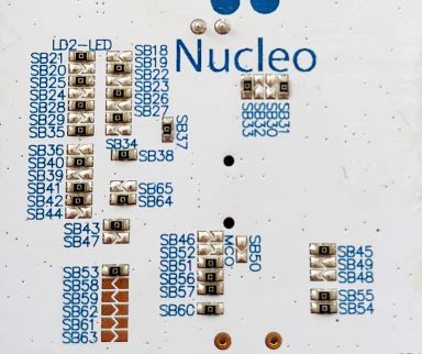
I did not check, but I guess for L4, SB37 is bridged, while SB34 is removed. Only for F37 with ths SDADC, SB34 is bridged and SB37 is removed.
- Mark as New
- Bookmark
- Subscribe
- Mute
- Subscribe to RSS Feed
- Permalink
- Email to a Friend
- Report Inappropriate Content
2020-02-13 01:56 AM
Thanks for your fast answer. But why is it bridged?
- Mark as New
- Bookmark
- Subscribe
- Mute
- Subscribe to RSS Feed
- Permalink
- Email to a Friend
- Report Inappropriate Content
2020-02-13 01:58 AM
I made a picture of the bridges:
- Mark as New
- Bookmark
- Subscribe
- Mute
- Subscribe to RSS Feed
- Permalink
- Email to a Friend
- Report Inappropriate Content
2020-02-13 02:02 AM
For the F37, you need SD_VREF on PB12. Otherwise you want PB12 to be accessible on the external connectors.
- Mark as New
- Bookmark
- Subscribe
- Mute
- Subscribe to RSS Feed
- Permalink
- Email to a Friend
- Report Inappropriate Content
2020-02-13 02:06 AM
My aim is to use the V_ref pin as input for external Voltage reference. I couldn't find any hints in data sheet why this connection is made. What happens fpr example when I don't connect it?
- Mark as New
- Bookmark
- Subscribe
- Mute
- Subscribe to RSS Feed
- Permalink
- Email to a Friend
- Report Inappropriate Content
2020-02-13 07:35 AM
Hello @FHopp.1 ,
You need to refer to AN4555 (Getting started with STM32L4 Series and STM32L4+ Series hardware development) where you will find following details:
The internal voltage reference buffer supports two output voltages, which are configured with VRS bit in the VREF_CSR register:
– VREF+ around 2.048 V. This requires VDDA equal to or higher than 2.4 V.
– VREF+ around 2.5 V. This requires VDDA equal to or higher than 2.8 V.
VREF- and VREF+ pins are not available on all packages. When not available, they are bonded to VSSA and VDDA, respectively.
When the VREF+ is double-bonded with VDDA in a package, the internal voltage reference buffer is not available and must be kept disable (refer to datasheet for packages pinout description).
VREF- must always be equal to VSSA.
So all depends on the package you selected and the availability of VREF+. You need to check the datasheet for such purpose.
-Amel
To give better visibility on the answered topics, please click on Accept as Solution on the reply which solved your issue or answered your question.
- Mark as New
- Bookmark
- Subscribe
- Mute
- Subscribe to RSS Feed
- Permalink
- Email to a Friend
- Report Inappropriate Content
2020-02-14 02:06 AM
Exectly. But this don't answer the question why V_ref/VDDA (Pin 13) is connected to PB12 (Pin 33) on the Nucleo Board. Why did ST do this?
- Mark as New
- Bookmark
- Subscribe
- Mute
- Subscribe to RSS Feed
- Permalink
- Email to a Friend
- Report Inappropriate Content
2020-02-14 07:29 AM
There is no SD_Vref+ for STM32L476. So when SB37 is bridged, this does not mean PB12 is connected to Vref+.
You need to look to SB57: it is ON which means "VDDA/VREF+ on STM32 is connected to VDD" (referring to UM1724).
-Amel
To give better visibility on the answered topics, please click on Accept as Solution on the reply which solved your issue or answered your question.
- Mark as New
- Bookmark
- Subscribe
- Mute
- Subscribe to RSS Feed
- Permalink
- Email to a Friend
- Report Inappropriate Content
2020-02-14 07:55 AM
OK, thanks!
- Overrun problem with USART2 in STM32H723 MCU in STM32 MCUs Embedded software
- Failed to execute MI Command in STM32 MCUs Products
- My board can no longer run the program I uploaded to it earlier in STM32CubeIDE (MCUs)
- ADCs - QUEUE in STM32 MCUs Products
- Why can't I create more than one TouchGFX projects connected to STM32CubeIDE? in STM32CubeIDE (MCUs)

