- STMicroelectronics Community
- STM32 MCUs
- STM32 MCUs Boards and hardware tools
- Re: Experiencing difficulties in creating a phase ...
- Subscribe to RSS Feed
- Mark Topic as New
- Mark Topic as Read
- Float this Topic for Current User
- Bookmark
- Subscribe
- Mute
- Printer Friendly Page
Experiencing difficulties in creating a phase difference between two PWM signals
- Mark as New
- Bookmark
- Subscribe
- Mute
- Subscribe to RSS Feed
- Permalink
- Email to a Friend
- Report Inappropriate Content
2023-09-11 06:22 PM
Hello everyone,
I'm new to using STM32 boards and coding with STM32CubeIDE. I have a simple task: generating two PWM outputs and adjusting the phase difference between these two PWM signals at runtime.
I'm using an STM32F407 board, and from what I've gathered through online research, I need to use two timers, one in master and another in slave configuration. For the master Timer (Timer 1), I've set up two PWM channels. Channel 1 of Timer 1 is for PWM generation, and Channel 2 of Timer 1 is for triggering Timer 2, which is set to 'output compare no output' mode. I followed a tutorial on YouTube (Timer Sync Tutorial ) to configure these channels.
The pulse value set in TIM1 CH2 is supposed to change the phase of the PWM generated by Timer 2. However, I'm unable to change the phase at runtime. I've tried changing the value of the CCR2 register in the main code, but it doesn't affect the phase despite updating CCR2.
Could someone please point out my mistake and provide the correct syntax? And if possible, could you explain it in simpler terms, as I'm relatively new to this?
/* USER CODE BEGIN Header */
/**
  ******************************************************************************
  * @file           : main.c
  * @brief          : Main program body
  ******************************************************************************
  * @attention
  *
  * Copyright (c) 2023 STMicroelectronics.
  * All rights reserved.
  *
  * This software is licensed under terms that can be found in the LICENSE file
  * in the root directory of this software component.
  * If no LICENSE file comes with this software, it is provided AS-IS.
  *
  ******************************************************************************
  */
/* USER CODE END Header */
/* Includes ------------------------------------------------------------------*/
#include "main.h"
#include "usb_host.h"

/* Private includes ----------------------------------------------------------*/
/* USER CODE BEGIN Includes */

/* USER CODE END Includes */

/* Private typedef -----------------------------------------------------------*/
/* USER CODE BEGIN PTD */

/* USER CODE END PTD */

/* Private define ------------------------------------------------------------*/
/* USER CODE BEGIN PD */

/* USER CODE END PD */

/* Private macro -------------------------------------------------------------*/
/* USER CODE BEGIN PM */

/* USER CODE END PM */

/* Private variables ---------------------------------------------------------*/
I2C_HandleTypeDef hi2c1;

I2S_HandleTypeDef hi2s3;

SPI_HandleTypeDef hspi1;

TIM_HandleTypeDef htim1;
TIM_HandleTypeDef htim2;

/* USER CODE BEGIN PV */

/* USER CODE END PV */

/* Private function prototypes -----------------------------------------------*/
void SystemClock_Config(void);
static void MX_GPIO_Init(void);
static void MX_I2C1_Init(void);
static void MX_I2S3_Init(void);
static void MX_SPI1_Init(void);
static void MX_TIM1_Init(void);
static void MX_TIM2_Init(void);
void MX_USB_HOST_Process(void);

/* USER CODE BEGIN PFP */

/* USER CODE END PFP */

/* Private user code ---------------------------------------------------------*/
/* USER CODE BEGIN 0 */

/* USER CODE END 0 */

/**
  * @brief  The application entry point.
  * @retval int
  */
int main(void)
{
  /* USER CODE BEGIN 1 */

  /* USER CODE END 1 */

  /* MCU Configuration--------------------------------------------------------*/

  /* Reset of all peripherals, Initializes the Flash interface and the Systick. */
  HAL_Init();

  /* USER CODE BEGIN Init */

  /* USER CODE END Init */

  /* Configure the system clock */
  SystemClock_Config();

  /* USER CODE BEGIN SysInit */

  /* USER CODE END SysInit */

  /* Initialize all configured peripherals */
  MX_GPIO_Init();
  MX_I2C1_Init();
  MX_I2S3_Init();
  MX_SPI1_Init();
  MX_USB_HOST_Init();
  MX_TIM1_Init();
  MX_TIM2_Init();
  /* USER CODE BEGIN 2 */
  HAL_TIM_PWM_Start(&htim1, TIM_CHANNEL_1);
  HAL_TIM_OC_Start(&htim1, TIM_CHANNEL_2);
  HAL_TIM_PWM_Start(&htim2, TIM_CHANNEL_1);
  /* USER CODE END 2 */

  /* Infinite loop */
  /* USER CODE BEGIN WHILE */
  while (1)
  {
    /* USER CODE END WHILE */
    MX_USB_HOST_Process();

    htim1.Instance->CCR2 =400;
    /* USER CODE BEGIN 3 */
  }
  /* USER CODE END 3 */
}

/**
  * @brief System Clock Configuration
  * @retval None
  */
void SystemClock_Config(void)
{
  RCC_OscInitTypeDef RCC_OscInitStruct = {0};
  RCC_ClkInitTypeDef RCC_ClkInitStruct = {0};

  /** Configure the main internal regulator output voltage
  */
  __HAL_RCC_PWR_CLK_ENABLE();
  __HAL_PWR_VOLTAGESCALING_CONFIG(PWR_REGULATOR_VOLTAGE_SCALE1);

  /** Initializes the RCC Oscillators according to the specified parameters
  * in the RCC_OscInitTypeDef structure.
  */
  RCC_OscInitStruct.OscillatorType = RCC_OSCILLATORTYPE_HSE;
  RCC_OscInitStruct.HSEState = RCC_HSE_ON;
  RCC_OscInitStruct.PLL.PLLState = RCC_PLL_ON;
  RCC_OscInitStruct.PLL.PLLSource = RCC_PLLSOURCE_HSE;
  RCC_OscInitStruct.PLL.PLLM = 8;
  RCC_OscInitStruct.PLL.PLLN = 336;
  RCC_OscInitStruct.PLL.PLLP = RCC_PLLP_DIV2;
  RCC_OscInitStruct.PLL.PLLQ = 7;
  if (HAL_RCC_OscConfig(&RCC_OscInitStruct) != HAL_OK)
  {
    Error_Handler();
  }

  /** Initializes the CPU, AHB and APB buses clocks
  */
  RCC_ClkInitStruct.ClockType = RCC_CLOCKTYPE_HCLK|RCC_CLOCKTYPE_SYSCLK
                              |RCC_CLOCKTYPE_PCLK1|RCC_CLOCKTYPE_PCLK2;
  RCC_ClkInitStruct.SYSCLKSource = RCC_SYSCLKSOURCE_PLLCLK;
  RCC_ClkInitStruct.AHBCLKDivider = RCC_SYSCLK_DIV1;
  RCC_ClkInitStruct.APB1CLKDivider = RCC_HCLK_DIV4;
  RCC_ClkInitStruct.APB2CLKDivider = RCC_HCLK_DIV4;

  if (HAL_RCC_ClockConfig(&RCC_ClkInitStruct, FLASH_LATENCY_5) != HAL_OK)
  {
    Error_Handler();
  }
}

/**
  * @brief I2C1 Initialization Function
  * @PAram None
  * @retval None
  */
static void MX_I2C1_Init(void)
{

  /* USER CODE BEGIN I2C1_Init 0 */

  /* USER CODE END I2C1_Init 0 */

  /* USER CODE BEGIN I2C1_Init 1 */

  /* USER CODE END I2C1_Init 1 */
  hi2c1.Instance = I2C1;
  hi2c1.Init.ClockSpeed = 100000;
  hi2c1.Init.DutyCycle = I2C_DUTYCYCLE_2;
  hi2c1.Init.OwnAddress1 = 0;
  hi2c1.Init.AddressingMode = I2C_ADDRESSINGMODE_7BIT;
  hi2c1.Init.DualAddressMode = I2C_DUALADDRESS_DISABLE;
  hi2c1.Init.OwnAddress2 = 0;
  hi2c1.Init.GeneralCallMode = I2C_GENERALCALL_DISABLE;
  hi2c1.Init.NoStretchMode = I2C_NOSTRETCH_DISABLE;
  if (HAL_I2C_Init(&hi2c1) != HAL_OK)
  {
    Error_Handler();
  }
  /* USER CODE BEGIN I2C1_Init 2 */

  /* USER CODE END I2C1_Init 2 */

}

/**
  * @brief I2S3 Initialization Function
  * @PAram None
  * @retval None
  */
static void MX_I2S3_Init(void)
{

  /* USER CODE BEGIN I2S3_Init 0 */

  /* USER CODE END I2S3_Init 0 */

  /* USER CODE BEGIN I2S3_Init 1 */

  /* USER CODE END I2S3_Init 1 */
  hi2s3.Instance = SPI3;
  hi2s3.Init.Mode = I2S_MODE_MASTER_TX;
  hi2s3.Init.Standard = I2S_STANDARD_PHILIPS;
  hi2s3.Init.DataFormat = I2S_DATAFORMAT_16B;
  hi2s3.Init.MCLKOutput = I2S_MCLKOUTPUT_ENABLE;
  hi2s3.Init.AudioFreq = I2S_AUDIOFREQ_96K;
  hi2s3.Init.CPOL = I2S_CPOL_LOW;
  hi2s3.Init.ClockSource = I2S_CLOCK_PLL;
  hi2s3.Init.FullDuplexMode = I2S_FULLDUPLEXMODE_DISABLE;
  if (HAL_I2S_Init(&hi2s3) != HAL_OK)
  {
    Error_Handler();
  }
  /* USER CODE BEGIN I2S3_Init 2 */

  /* USER CODE END I2S3_Init 2 */

}

/**
  * @brief SPI1 Initialization Function
  * @PAram None
  * @retval None
  */
static void MX_SPI1_Init(void)
{

  /* USER CODE BEGIN SPI1_Init 0 */

  /* USER CODE END SPI1_Init 0 */

  /* USER CODE BEGIN SPI1_Init 1 */

  /* USER CODE END SPI1_Init 1 */
  /* SPI1 parameter configuration*/
  hspi1.Instance = SPI1;
  hspi1.Init.Mode = SPI_MODE_MASTER;
  hspi1.Init.Direction = SPI_DIRECTION_2LINES;
  hspi1.Init.DataSize = SPI_DATASIZE_8BIT;
  hspi1.Init.CLKPolarity = SPI_POLARITY_LOW;
  hspi1.Init.CLKPhase = SPI_PHASE_1EDGE;
  hspi1.Init.NSS = SPI_NSS_SOFT;
  hspi1.Init.BaudRatePrescaler = SPI_BAUDRATEPRESCALER_2;
  hspi1.Init.FirstBit = SPI_FIRSTBIT_MSB;
  hspi1.Init.TIMode = SPI_TIMODE_DISABLE;
  hspi1.Init.CRCCalculation = SPI_CRCCALCULATION_DISABLE;
  hspi1.Init.CRCPolynomial = 10;
  if (HAL_SPI_Init(&hspi1) != HAL_OK)
  {
    Error_Handler();
  }
  /* USER CODE BEGIN SPI1_Init 2 */

  /* USER CODE END SPI1_Init 2 */

}

/**
  * @brief TIM1 Initialization Function
  * @PAram None
  * @retval None
  */
static void MX_TIM1_Init(void)
{

  /* USER CODE BEGIN TIM1_Init 0 */

  /* USER CODE END TIM1_Init 0 */

  TIM_MasterConfigTypeDef sMasterConfig = {0};
  TIM_OC_InitTypeDef sConfigOC = {0};
  TIM_BreakDeadTimeConfigTypeDef sBreakDeadTimeConfig = {0};

  /* USER CODE BEGIN TIM1_Init 1 */

  /* USER CODE END TIM1_Init 1 */
  htim1.Instance = TIM1;
  htim1.Init.Prescaler = 0;
  htim1.Init.CounterMode = TIM_COUNTERMODE_UP;
  htim1.Init.Period = 989;
  htim1.Init.ClockDivision = TIM_CLOCKDIVISION_DIV1;
  htim1.Init.RepetitionCounter = 0;
  htim1.Init.AutoReloadPreload = TIM_AUTORELOAD_PRELOAD_DISABLE;
  if (HAL_TIM_PWM_Init(&htim1) != HAL_OK)
  {
    Error_Handler();
  }
  if (HAL_TIM_OC_Init(&htim1) != HAL_OK)
  {
    Error_Handler();
  }
  sMasterConfig.MasterOutputTrigger = TIM_TRGO_OC2REF;
  sMasterConfig.MasterSlaveMode = TIM_MASTERSLAVEMODE_DISABLE;
  if (HAL_TIMEx_MasterConfigSynchronization(&htim1, &sMasterConfig) != HAL_OK)
  {
    Error_Handler();
  }
  sConfigOC.OCMode = TIM_OCMODE_PWM1;
  sConfigOC.Pulse = 494;
  sConfigOC.OCPolarity = TIM_OCPOLARITY_HIGH;
  sConfigOC.OCNPolarity = TIM_OCNPOLARITY_HIGH;
  sConfigOC.OCFastMode = TIM_OCFAST_DISABLE;
  sConfigOC.OCIdleState = TIM_OCIDLESTATE_RESET;
  sConfigOC.OCNIdleState = TIM_OCNIDLESTATE_RESET;
  if (HAL_TIM_PWM_ConfigChannel(&htim1, &sConfigOC, TIM_CHANNEL_1) != HAL_OK)
  {
    Error_Handler();
  }
  sConfigOC.OCMode = TIM_OCMODE_ACTIVE;
  sConfigOC.Pulse = 247;
  if (HAL_TIM_OC_ConfigChannel(&htim1, &sConfigOC, TIM_CHANNEL_2) != HAL_OK)
  {
    Error_Handler();
  }
  __HAL_TIM_ENABLE_OCxPRELOAD(&htim1, TIM_CHANNEL_2);
  sBreakDeadTimeConfig.OffStateRunMode = TIM_OSSR_DISABLE;
  sBreakDeadTimeConfig.OffStateIDLEMode = TIM_OSSI_DISABLE;
  sBreakDeadTimeConfig.LockLevel = TIM_LOCKLEVEL_OFF;
  sBreakDeadTimeConfig.DeadTime = 0;
  sBreakDeadTimeConfig.BreakState = TIM_BREAK_DISABLE;
  sBreakDeadTimeConfig.BreakPolarity = TIM_BREAKPOLARITY_HIGH;
  sBreakDeadTimeConfig.AutomaticOutput = TIM_AUTOMATICOUTPUT_DISABLE;
  if (HAL_TIMEx_ConfigBreakDeadTime(&htim1, &sBreakDeadTimeConfig) != HAL_OK)
  {
    Error_Handler();
  }
  /* USER CODE BEGIN TIM1_Init 2 */

  /* USER CODE END TIM1_Init 2 */
  HAL_TIM_MspPostInit(&htim1);

}

/**
  * @brief TIM2 Initialization Function
  * @PAram None
  * @retval None
  */
static void MX_TIM2_Init(void)
{

  /* USER CODE BEGIN TIM2_Init 0 */

  /* USER CODE END TIM2_Init 0 */

  TIM_SlaveConfigTypeDef sSlaveConfig = {0};
  TIM_MasterConfigTypeDef sMasterConfig = {0};
  TIM_OC_InitTypeDef sConfigOC = {0};

  /* USER CODE BEGIN TIM2_Init 1 */

  /* USER CODE END TIM2_Init 1 */
  htim2.Instance = TIM2;
  htim2.Init.Prescaler = 0;
  htim2.Init.CounterMode = TIM_COUNTERMODE_UP;
  htim2.Init.Period = 989;
  htim2.Init.ClockDivision = TIM_CLOCKDIVISION_DIV1;
  htim2.Init.AutoReloadPreload = TIM_AUTORELOAD_PRELOAD_DISABLE;
  if (HAL_TIM_Base_Init(&htim2) != HAL_OK)
  {
    Error_Handler();
  }
  if (HAL_TIM_PWM_Init(&htim2) != HAL_OK)
  {
    Error_Handler();
  }
  sSlaveConfig.SlaveMode = TIM_SLAVEMODE_TRIGGER;
  sSlaveConfig.InputTrigger = TIM_TS_ITR0;
  if (HAL_TIM_SlaveConfigSynchro(&htim2, &sSlaveConfig) != HAL_OK)
  {
    Error_Handler();
  }
  sMasterConfig.MasterOutputTrigger = TIM_TRGO_OC2REF;
  sMasterConfig.MasterSlaveMode = TIM_MASTERSLAVEMODE_DISABLE;
  if (HAL_TIMEx_MasterConfigSynchronization(&htim2, &sMasterConfig) != HAL_OK)
  {
    Error_Handler();
  }
  sConfigOC.OCMode = TIM_OCMODE_PWM1;
  sConfigOC.Pulse = 494;
  sConfigOC.OCPolarity = TIM_OCPOLARITY_HIGH;
  sConfigOC.OCFastMode = TIM_OCFAST_DISABLE;
  if (HAL_TIM_PWM_ConfigChannel(&htim2, &sConfigOC, TIM_CHANNEL_1) != HAL_OK)
  {
    Error_Handler();
  }
  /* USER CODE BEGIN TIM2_Init 2 */

  /* USER CODE END TIM2_Init 2 */
  HAL_TIM_MspPostInit(&htim2);

}

/**
  * @brief GPIO Initialization Function
  * @PAram None
  * @retval None
  */
static void MX_GPIO_Init(void)
{
  GPIO_InitTypeDef GPIO_InitStruct = {0};
/* USER CODE BEGIN MX_GPIO_Init_1 */
/* USER CODE END MX_GPIO_Init_1 */

  /* GPIO Ports Clock Enable */
  __HAL_RCC_GPIOE_CLK_ENABLE();
  __HAL_RCC_GPIOC_CLK_ENABLE();
  __HAL_RCC_GPIOH_CLK_ENABLE();
  __HAL_RCC_GPIOA_CLK_ENABLE();
  __HAL_RCC_GPIOB_CLK_ENABLE();
  __HAL_RCC_GPIOD_CLK_ENABLE();

  /*Configure GPIO pin Output Level */
  HAL_GPIO_WritePin(CS_I2C_SPI_GPIO_Port, CS_I2C_SPI_Pin, GPIO_PIN_RESET);

  /*Configure GPIO pin Output Level */
  HAL_GPIO_WritePin(OTG_FS_PowerSwitchOn_GPIO_Port, OTG_FS_PowerSwitchOn_Pin, GPIO_PIN_SET);

  /*Configure GPIO pin Output Level */
  HAL_GPIO_WritePin(GPIOD, LD4_Pin|LD3_Pin|LD5_Pin|LD6_Pin
                          |Audio_RST_Pin, GPIO_PIN_RESET);

  /*Configure GPIO pin : CS_I2C_SPI_Pin */
  GPIO_InitStruct.Pin = CS_I2C_SPI_Pin;
  GPIO_InitStruct.Mode = GPIO_MODE_OUTPUT_PP;
  GPIO_InitStruct.Pull = GPIO_NOPULL;
  GPIO_InitStruct.Speed = GPIO_SPEED_FREQ_LOW;
  HAL_GPIO_Init(CS_I2C_SPI_GPIO_Port, &GPIO_InitStruct);

  /*Configure GPIO pin : OTG_FS_PowerSwitchOn_Pin */
  GPIO_InitStruct.Pin = OTG_FS_PowerSwitchOn_Pin;
  GPIO_InitStruct.Mode = GPIO_MODE_OUTPUT_PP;
  GPIO_InitStruct.Pull = GPIO_NOPULL;
  GPIO_InitStruct.Speed = GPIO_SPEED_FREQ_LOW;
  HAL_GPIO_Init(OTG_FS_PowerSwitchOn_GPIO_Port, &GPIO_InitStruct);

  /*Configure GPIO pin : PDM_OUT_Pin */
  GPIO_InitStruct.Pin = PDM_OUT_Pin;
  GPIO_InitStruct.Mode = GPIO_MODE_AF_PP;
  GPIO_InitStruct.Pull = GPIO_NOPULL;
  GPIO_InitStruct.Speed = GPIO_SPEED_FREQ_LOW;
  GPIO_InitStruct.Alternate = GPIO_AF5_SPI2;
  HAL_GPIO_Init(PDM_OUT_GPIO_Port, &GPIO_InitStruct);

  /*Configure GPIO pin : B1_Pin */
  GPIO_InitStruct.Pin = B1_Pin;
  GPIO_InitStruct.Mode = GPIO_MODE_EVT_RISING;
  GPIO_InitStruct.Pull = GPIO_NOPULL;
  HAL_GPIO_Init(B1_GPIO_Port, &GPIO_InitStruct);

  /*Configure GPIO pin : BOOT1_Pin */
  GPIO_InitStruct.Pin = BOOT1_Pin;
  GPIO_InitStruct.Mode = GPIO_MODE_INPUT;
  GPIO_InitStruct.Pull = GPIO_NOPULL;
  HAL_GPIO_Init(BOOT1_GPIO_Port, &GPIO_InitStruct);

  /*Configure GPIO pin : CLK_IN_Pin */
  GPIO_InitStruct.Pin = CLK_IN_Pin;
  GPIO_InitStruct.Mode = GPIO_MODE_AF_PP;
  GPIO_InitStruct.Pull = GPIO_NOPULL;
  GPIO_InitStruct.Speed = GPIO_SPEED_FREQ_LOW;
  GPIO_InitStruct.Alternate = GPIO_AF5_SPI2;
  HAL_GPIO_Init(CLK_IN_GPIO_Port, &GPIO_InitStruct);

  /*Configure GPIO pins : LD4_Pin LD3_Pin LD5_Pin LD6_Pin
                           Audio_RST_Pin */
  GPIO_InitStruct.Pin = LD4_Pin|LD3_Pin|LD5_Pin|LD6_Pin
                          |Audio_RST_Pin;
  GPIO_InitStruct.Mode = GPIO_MODE_OUTPUT_PP;
  GPIO_InitStruct.Pull = GPIO_NOPULL;
  GPIO_InitStruct.Speed = GPIO_SPEED_FREQ_LOW;
  HAL_GPIO_Init(GPIOD, &GPIO_InitStruct);

  /*Configure GPIO pin : OTG_FS_OverCurrent_Pin */
  GPIO_InitStruct.Pin = OTG_FS_OverCurrent_Pin;
  GPIO_InitStruct.Mode = GPIO_MODE_INPUT;
  GPIO_InitStruct.Pull = GPIO_NOPULL;
  HAL_GPIO_Init(OTG_FS_OverCurrent_GPIO_Port, &GPIO_InitStruct);

  /*Configure GPIO pin : MEMS_INT2_Pin */
  GPIO_InitStruct.Pin = MEMS_INT2_Pin;
  GPIO_InitStruct.Mode = GPIO_MODE_EVT_RISING;
  GPIO_InitStruct.Pull = GPIO_NOPULL;
  HAL_GPIO_Init(MEMS_INT2_GPIO_Port, &GPIO_InitStruct);

/* USER CODE BEGIN MX_GPIO_Init_2 */
/* USER CODE END MX_GPIO_Init_2 */
}

/* USER CODE BEGIN 4 */

/* USER CODE END 4 */

/**
  * @brief  This function is executed in case of error occurrence.
  * @retval None
  */
void Error_Handler(void)
{
  /* USER CODE BEGIN Error_Handler_Debug */
  /* User can add his own implementation to report the HAL error return state */
  __disable_irq();
  while (1)
  {
  }
  /* USER CODE END Error_Handler_Debug */
}

#ifdef  USE_FULL_ASSERT
/**
  * @brief  Reports the name of the source file and the source line number
  *         where the assert_param error has occurred.
  * @PAram  file: pointer to the source file name
  * @PAram  line: assert_param error line source number
  * @retval None
  */
void assert_failed(uint8_t *file, uint32_t line)
{
  /* USER CODE BEGIN 6 */
  /* User can add his own implementation to report the file name and line number,
     ex: printf("Wrong parameters value: file %s on line %d\r\n", file, line) */
  /* USER CODE END 6 */
}
#endif /* USE_FULL_ASSERT */- Labels:
-
STM32F4 Series
- Mark as New
- Bookmark
- Subscribe
- Mute
- Subscribe to RSS Feed
- Permalink
- Email to a Friend
- Report Inappropriate Content
2023-09-11 06:54 PM - edited 2023-09-11 06:55 PM
Hello @SKhan.16
I have an easy way to do this. First, create 2 PWM with exactly the same characteristics. Then create a counter using another TIMER channel to count for the half of the period of the pwm signals(∆T/2). After that:
- Start generating your first PWM.
- Start the counter.
- When the counter end counting, use the interruption to start the second pwm.
Now, for your code you need to stop the pwm generation and the output compare timer, change your CCR2 value and then restart them.
Best regards.
II
- Mark as New
- Bookmark
- Subscribe
- Mute
- Subscribe to RSS Feed
- Permalink
- Email to a Friend
- Report Inappropriate Content
2023-09-11 08:34 PM - edited 2023-09-11 08:34 PM
Dear @Issamos,
Thank you very much for your prompt response. As I mentioned earlier, I'm quite new to STM32, and my experience is somewhat limited.
So, if I understand correctly, you're suggesting that I configure another TIMER, let's say TIMER 3, and have TIMER3 control the start of TIMER2 in a manner similar to what I've done in my existing program?
However, shouldn't there be a simpler way to allow TIMER1's CCR2 to modify the counter of TIMER2 during runtime in the main() function? After all, they are in a master-slave configuration with the trigger event set to OC2REF. For instance:
          HAL_Delay(1000);
          htim1.Instance->CCR2=200;
          HAL_Delay(1000);
          htim1.Instance->CCR2=400;
- Mark as New
- Bookmark
- Subscribe
- Mute
- Subscribe to RSS Feed
- Permalink
- Email to a Friend
- Report Inappropriate Content
2023-09-11 08:49 PM - edited 2023-09-11 10:11 PM
Additionally, if I adjust the duty cycle of both PWM channels by modifying CCR1 during runtime, I can see the duty cycle changes, indicating that CCR1 is being updated dynamically. However, I've encountered an issue with CCR2; it doesn't seem to update. I suspect I might be overlooking something, but I haven't been able to identify the problem so far.
 while (1)
  {
    MX_USB_HOST_Process();
              HAL_Delay(1000);
              htim1.Instance->CCR1 =494;
              htim2.Instance->CCR1 =494;
              htim1.Instance->CCR2 =494;

              HAL_Delay(1000);
              htim1.Instance->CCR1 =247;
              htim2.Instance->CCR1 =247;
              htim1.Instance->CCR2 =247;
  }
- Mark as New
- Bookmark
- Subscribe
- Mute
- Subscribe to RSS Feed
- Permalink
- Email to a Friend
- Report Inappropriate Content
2023-09-12 03:38 AM - edited 2023-09-12 03:39 AM
Hello @SKhan.16,
This video will give you a better understanding of the internal triggering system with a demo.
Also, you may want to check paragraph Timer synchronization in the reference manual for more details.
To give better visibility on the answered topics, please click on Accept as Solution on the reply which solved your issue or answered your question.
- Mark as New
- Bookmark
- Subscribe
- Mute
- Subscribe to RSS Feed
- Permalink
- Email to a Friend
- Report Inappropriate Content
2023-09-12 03:51 AM
Trigger mode of slave-mode controller works so, that when trigger arrives, it sets TIMx_CR1.CEN (i.e. enables the counter). Once the counter is enabled, it does nothing, so it can't cause any magic resynchronization.
So, there are two ways to do this: either set the slave timer to one-pulse mode (i.e. set TIMx_CR1.OPM=1), that clears TIMx_CR1.CEN after every Update (overflow) allowing the master to start it again; but in that case you want also set the slave timer's period (ARR) somewhat shorter than the master's. Alternatively, leave the slave timer running freely (i.e. TIMx_CR1.OPM=0), but change the slave-mode controller's mode to Reset.
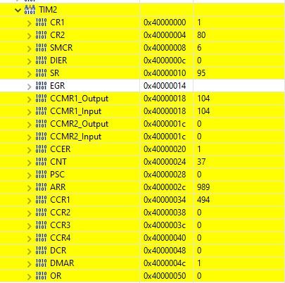
Why your TIM1_CH2 change won't work I don't know, but whatever you do, start with reading out and checking/posting the TIM registers content.
JW
- Mark as New
- Bookmark
- Subscribe
- Mute
- Subscribe to RSS Feed
- Permalink
- Email to a Friend
- Report Inappropriate Content
2023-09-13 02:10 AM
Dear @Sarra.S ,
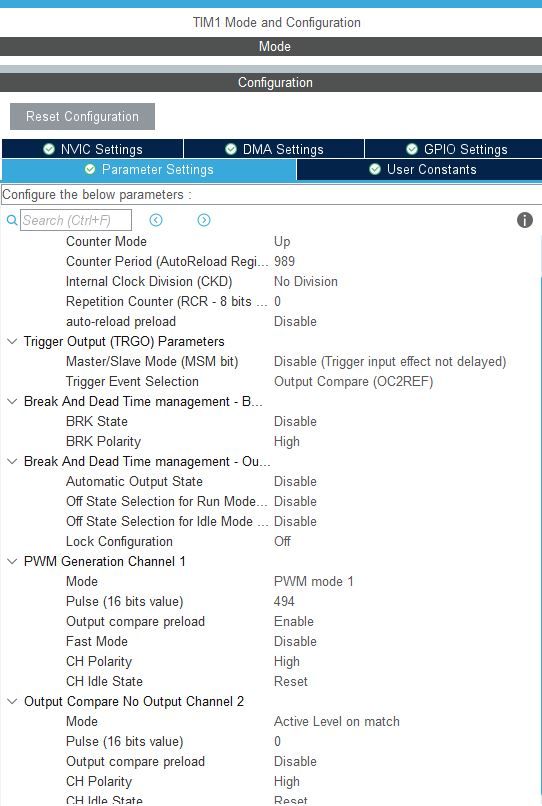
Thank you for your response. I have already watched this video. The phase of TIM2's PWM1 is delayed if I set the pulse of TIM1's CH2 in the Pinout and Configuration section of STM32CubeIDE. However, the phase does not change if I modify "htim1.Instance->CCR2" in the main function. This is the problem I am facing. I want to update "htim1.Instance->CCR2" during runtime.
Dear @waclawek.jan ,
Thank you for your detailed answer. I followed your methods, but none of them solved the problem. I also set up another timer, TIM3, as the master for TIM2 and set TIM3 CH1 as "output compare no output," following the settings from the reference manual of STM32F407. However, that did not help.
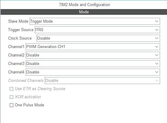
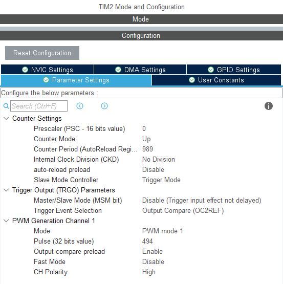
Attached are the screenshots of TIMx and CHx configurations along with register values. I still cannot figure out why I am facing this problem, even though I have tried almost everything I could find on the internet. So far, I have not found any demonstrations of varying phase shifts in runtime. What should I do?


- Mark as New
- Bookmark
- Subscribe
- Mute
- Subscribe to RSS Feed
- Permalink
- Email to a Friend
- Report Inappropriate Content
2023-09-13 02:24 AM
TIM1->CR2 = 0x80 means TIM1_CR2.MMS = 0b000 which is different from what you want, which is probably TIM1_CR2.MMS=0b101 (Compare - OC2REF signal is used as trigger output (TRGO)).
I don't use CubeMX nor Cube/HAL and I am not interested in finding reasons why it does not work as intended. IMO timers are simple enough to be programmed normally through direct register access.
JW
- STM32CubeIDE Compile Time using Linux is VERY SLOW in STM32CubeIDE (MCUs)
- How to integrate STM32 Extension to DevContainer in STM32 VSCode extension (MCUs)
- "Upgrade error, please try again" with ST-Link in STM32 MCUs Products
- STM32G431 Custom Control Board Noisy Current Sense in STM32 MCUs Motor control
- STM32H7B3 Issue: Low voltage from USB Power Supply and Inaccessible BOOT0 Pin in STM32 MCUs Boards and hardware tools