- STMicroelectronics Community
- STM32 MCUs
- STM32 MCUs Boards and hardware tools
- Value gaps in DMA transferred ADC data
- Subscribe to RSS Feed
- Mark Topic as New
- Mark Topic as Read
- Float this Topic for Current User
- Bookmark
- Subscribe
- Mute
- Printer Friendly Page
Value gaps in DMA transferred ADC data
- Mark as New
- Bookmark
- Subscribe
- Mute
- Subscribe to RSS Feed
- Permalink
- Email to a Friend
- Report Inappropriate Content
2022-03-31 6:09 AM
Setup is as follows:
ADC1 & 2 in 'Dual regular simultaneous mode only'
DMA1 stream 0 used to transfer ADC data to AXI SRAM buffer (40000 32 bit values), DMA circular mode.
Using 'HAL_ADC_ConvHalfCpltCallback' to signal half buffer filled and 'HAL_ADC_ConvCpltCallback' to signal full buffer.
When the second half is filling, the first half is processed by application and vice versa.
This basically works good but buffer data for ADC 1 shows gaps at even 4k levels.
Example: Imagine the rising part of a triangle wave signal at ADC inputs. Simplified data example below.
ADC1 ADC2
---- ----
4092 4092
4093 4093
4094 4094
4095 4095
4095 4096
4095 4097
-
-
-
4095 4194
4095 4195
4095 4196
4197 4197
4198 4198
etc.
At 4095, 8191, 12287 and so on with 4k intervals, data in buffer from ADC1 gets "stuck" for a while and then continues with a jump.
What could be the reason?
- Labels:
-
ADC
-
DMA
-
STM32H7 series
- Mark as New
- Bookmark
- Subscribe
- Mute
- Subscribe to RSS Feed
- Permalink
- Email to a Friend
- Report Inappropriate Content
2022-03-31 6:12 AM
Which STM32?
> What could be the reason?
Unstable reference(VREF+).
JW
Recent thread with similar question:
https://community.st.com/s/question/0D53W00001ScZlJSAV/adc-output-with-offset-in-some-unknown-region
- Mark as New
- Bookmark
- Subscribe
- Mute
- Subscribe to RSS Feed
- Permalink
- Email to a Friend
- Report Inappropriate Content
2022-03-31 6:52 AM
Custom board? How is VDDA/VREF+ wired exactly? Agree that VREF+ seems like the issue, likely insufficient capacitance.
https://community.st.com/s/question/0D53W0000082ShTSAU/stm32f401-adc-not-getting-all-the-values
- Mark as New
- Bookmark
- Subscribe
- Mute
- Subscribe to RSS Feed
- Permalink
- Email to a Friend
- Report Inappropriate Content
2022-04-01 12:00 AM
I looked at both links, and they seem to describe both the problem and the solution.
This is a custom board.

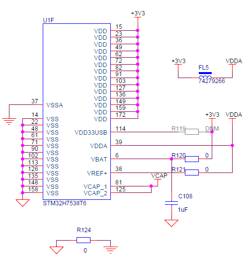
VREF+ and VDDA are tied together and derived from +3V3 via an EMI filter, without any capacitor.
I will test with a capacitor added.
- Mark as New
- Bookmark
- Subscribe
- Mute
- Subscribe to RSS Feed
- Permalink
- Email to a Friend
- Report Inappropriate Content
2022-04-12 2:40 AM
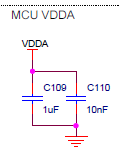
The VDDA/VREF+ pins actually had capacitors, they were in another corner of the circuit diagram:

quite airight, no long tracks etc.
I have also tested a number of different settings including different ADC bit resolution, ADC clock prescaler and all available ADCs_Common_Settings.
Even if I set ADC1 to 'Independent mode' the problem remains.
- Mark as New
- Bookmark
- Subscribe
- Mute
- Subscribe to RSS Feed
- Permalink
- Email to a Friend
- Report Inappropriate Content
2022-04-13 1:20 AM
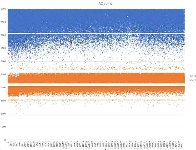
ADC data gaps:

The horizontal white stripes thus representing gaps in ADC data.
The ADC1 graph shows gaps at 4k intervals (it continues at 8191, 12287 and so on) but the ADC2 graph
shows intervals of 512 and there are nearly 25% of "dead" values for the orange plot.
This data comes from a third unit I tested, and fact is that all three differ in behaviour even if they run the same program.
The other two does not display any dead data for ADC2, but they differ in the ADC1 interval; one has 4k intervals the other has 16k intervals.
So the problem seems to differ between different MCU units.
Building on the above, I'm shifting focus towards the ADC setup.
- Mark as New
- Bookmark
- Subscribe
- Mute
- Subscribe to RSS Feed
- Permalink
- Email to a Friend
- Report Inappropriate Content
2022-10-14 6:05 AM
Problem solved (been ignored for a while).
The ADC:s must be calibrated before startup, which they weren't.
After running
HAL_ADCEx_Calibration_Start(&hadc1, ADC_CALIB_OFFSET_LINEARITY, ADC_SINGLE_ENDED)
last in MX_ADC1_Init for ADC1 the problem seems to have disappeared.
Do this for each ADC used.
Read about the calibration in documents AN5354 and RM0433 ADC Calibration section.
- Mark as New
- Bookmark
- Subscribe
- Mute
- Subscribe to RSS Feed
- Permalink
- Email to a Friend
- Report Inappropriate Content
2022-10-14 6:48 AM
This is very interesting.
Thanks for coming back with the finding.
JW
- Request for Guidance on Software-Only Firmware Update Mechanism through USB in STM32 MCUs Embedded software
- I2C with repeated start. in STM32 MCUs Products
- slow data rate with usb cdc on nucleo-h533 in STM32 MCUs Embedded software
- TSDHD STM32H7S7I8T6 in Others: STM32 MCUs related
- Continuous Reboot Issue with STM32G070CBT6 in STM32 MCUs Products