- STMicroelectronics Community
- STM32 MCUs
- STM32 MCUs Products
- ADC output with offset in some unknown region
- Subscribe to RSS Feed
- Mark Topic as New
- Mark Topic as Read
- Float this Topic for Current User
- Bookmark
- Subscribe
- Mute
- Printer Friendly Page
ADC output with offset in some unknown region
- Mark as New
- Bookmark
- Subscribe
- Mute
- Subscribe to RSS Feed
- Permalink
- Email to a Friend
- Report Inappropriate Content
2022-03-28 11:17 PM
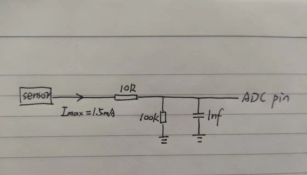
We are migrating project from F303 to G473, but the ADC output of G473 confused us with a strange problem, and with same circuit with F303 project below:

sampling period: 1.16us
voltage range: 1~3V
Vdda / Vref: 3.3V
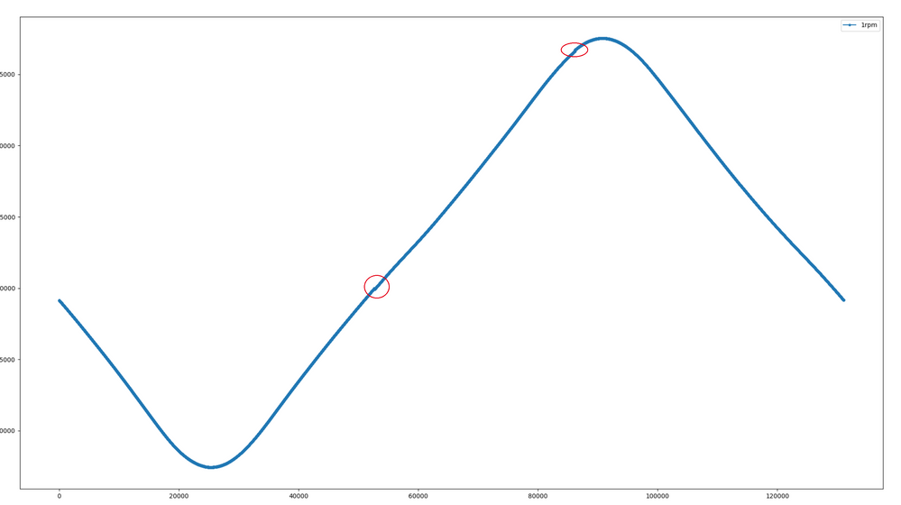
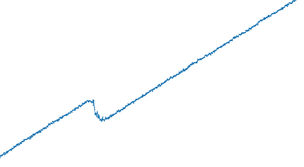
Here is thre problem curve output from ADC, the range between this two ramping point got a negative offset from original curve:


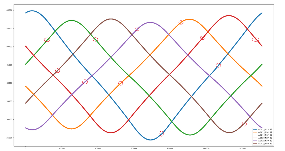
The output from six channels from dual ADC show that the problem presented randomly.

Although increasing the sampling time could cover the problem, but the sampling period is too long, we think it's not the right solution, since we used almost same sampling time on F303 project and works fine.
So what's the functional difference between F3 and G4 will cause this problem and how we solve this?
- Labels:
-
ADC
-
STM32F3 Series
-
STM32G4 Series
- Mark as New
- Bookmark
- Subscribe
- Mute
- Subscribe to RSS Feed
- Permalink
- Email to a Friend
- Report Inappropriate Content
2022-03-29 6:21 AM
Is VDDA/VREF+ stable with sufficient capacitance on the line?
How far away are the sensors and does the behavior change if you alter how the wires between them run?
If you measure a constant voltage which is generated close to the chip (e.g. 1.5V), is the problem present there as well?
- Mark as New
- Bookmark
- Subscribe
- Mute
- Subscribe to RSS Feed
- Permalink
- Email to a Friend
- Report Inappropriate Content
2022-03-29 6:49 AM
Also, read AN5346.
JW
- TouchGFX Application Shows Black Screen After Bootloader Jump in STM32 MCUs TouchGFX and GUI
- Linking errors in basic STM32WBA ZigBee OnOff-Server project in STM32CubeIDE for Visual Studio Code (MCUs)
- VSCode /ninja Linker failure with imported example code - XSPI_PSRAM_MemoryMapped in STM32CubeIDE for Visual Studio Code (MCUs)
- STM32N6 RIF and MMT autoconfiguration errors in STM32CubeMX (MCUs)
- system_stm32wb0x.c - dangerous relocation: unsupported relocation in STM32CubeMX (MCUs)
