- STMicroelectronics Community
- STM32 MPUs
- STM32 MPUs Boards and hardware tools
- How to allocate/multiplex GPIO specifically to Cor...
- Subscribe to RSS Feed
- Mark Topic as New
- Mark Topic as Read
- Float this Topic for Current User
- Bookmark
- Subscribe
- Mute
- Printer Friendly Page
How to allocate/multiplex GPIO specifically to Cortex-M4?
- Mark as New
- Bookmark
- Subscribe
- Mute
- Subscribe to RSS Feed
- Permalink
- Email to a Friend
- Report Inappropriate Content
2020-02-04 7:11 AM
Hi, I am currently looking at how to enable a GPIO pin on the M4 with the MP157A-DK1 kit.
In the datasheet it is unclear to me how I can assign the gpio pin specifically to one of the two processors (A7 or M4) or is this not necessary?
Thanks,
Rens
- Labels:
-
GPIO-EXTI
-
ST-Boards
-
STM32MP15 Lines
- Mark as New
- Bookmark
- Subscribe
- Mute
- Subscribe to RSS Feed
- Permalink
- Email to a Friend
- Report Inappropriate Content
2020-02-04 7:26 AM
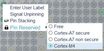
Once GPIO is set in CubeMx, use Right-Click to assign to Cortex-M4.
This will ensure the generated code is present in main.c
Regards
- Mark as New
- Bookmark
- Subscribe
- Mute
- Subscribe to RSS Feed
- Permalink
- Email to a Friend
- Report Inappropriate Content
2020-02-07 4:46 AM
Hi Patrick,
Thanks for your quick reply.
For my use case it's preferable to work without CubeMx.
I currently managed to get the IO pin to toggle via the M4.
For this I did not have to do anything besides running my program on the M4.
How is the multiplexing managed between the A7 and the M4?
- Mark as New
- Bookmark
- Subscribe
- Mute
- Subscribe to RSS Feed
- Permalink
- Email to a Friend
- Report Inappropriate Content
2020-02-07 5:13 AM
please have a look to https://wiki.st.com/stm32mpu/wiki/GPIO_internal_peripheral
- Mark as New
- Bookmark
- Subscribe
- Mute
- Subscribe to RSS Feed
- Permalink
- Email to a Friend
- Report Inappropriate Content
2020-02-10 7:47 AM
Hi Patrick,
I managed to get the GPIO pin working, however there are still some things unclear to me.
I wanted to test the maximal speed for a pintoggle using C code. without code optimization using the following code:
uint32_t pin11 = (uint32_t) GPIO_PIN_11;
  while (1)
  {
	GPIOA->BRR = pin11;
	GPIOA->BSRR = pin11;
  }
This produces the following assembly code:
;while(1)
.L3:
       ;GPIO->BRR=GPIO_PIN_11
        ldr     r2, .L4+4
        ldr     r3, [r7, #4]
        str     r3, [r2, #40]
        ;GPIO->BSRR=GPIO_PIN_11
        ldr     r2, .L4+4
        ldr     r3, [r7, #4]
        str     r3, [r2, #24]

        b       .L3
I used the arm reference manuals to calculate that this should take 14 instruction cycles to execute.
I think that on the oscilloscope it should display an uneven square wave, due to the execution time of the branch instruction. (2 instructions presumably?)
When probing the gpio_pin_11 i see an even square wave with a period of 86,4ns, thus 18 instructions.
Is there any reasonable explanation for this? :)
- Mark as New
- Bookmark
- Subscribe
- Mute
- Subscribe to RSS Feed
- Permalink
- Email to a Friend
- Report Inappropriate Content
2020-02-10 8:08 AM
ARM reference manual assume 0 delay in the interconnect, which is not true all time.
As there is some 'default slave' decoding in the AHB matrix, performance on the data (i.e. "ldr r2, .L4+4") depend on Cortex-M4 bus usage.
SRAM2 using S-Bus (i.e. starting @0x30020000) or RETRAM using D-Bus (starting @0x00000000) are recommend to avoid 1 cycle penalty for data.
I'm not sure the branch add a penalty as it is fetch on I-Bus while the store is done using S-Bus.
The access to the GPIO is maybe not 0 wait state.
Overall, best performance usually require to use a different memory/bus for code and data.
Maybe you could try using the following mapping:
- Code in SRAM1 @0x10000000 (so, using I-Bus)
- Data in RETRAM @0x00000000 (so, using D-Bus)
- GPIO control will use S-Bus
- Mark as New
- Bookmark
- Subscribe
- Mute
- Subscribe to RSS Feed
- Permalink
- Email to a Friend
- Report Inappropriate Content
2020-11-18 8:00 PM
You didn't have to modify your device tree at all? I'm currently trying to do the same thing and CubeMX is just generating GPIO definitions for the M4 and seems content to not touch the devicetree file. I haven't tried it yet, because I had kind of assumed that there would be DTS modifications needed...
- "How to create your own machine" in wiki and hits optee CFG_DRAM_SIZE bug in STM32 MPUs Products
- Core1 Wake-up Issue During SD Card Boot on STM32MP257 in STM32 MPUs Products
- AI model for stm32Mp157(cortexM4) in STM32 MPUs Products
- Quantized Gemma Model Inference on STM32MP257F-DK Board in STM32 MPUs Embedded software and solutions
- STM32MP257DAI3 and LPDDR4 Impedance Recommendation in STM32 MPUs Products
