- STMicroelectronics Community
- Knowledge base
- STM32 MCUs
- How to set up the OSPI peripheral to interface wit...
- Subscribe to RSS Feed
- Mark as New
- Mark as Read
- Bookmark
- Subscribe
- Email to a Friend
- Printer Friendly Page
- Report Inappropriate Content
How to set up the OSPI peripheral to interface with the IS25LX256 from ISSI
- Subscribe to RSS Feed
- Mark as New
- Mark as Read
- Bookmark
- Subscribe
- Email to a Friend
- Printer Friendly Page
- Report Inappropriate Content
on
2023-03-01
11:36 PM
- edited on
2024-06-10
2:47 AM
by
![]() Laurids_PETERSE
Laurids_PETERSE
Introduction
It is very common for HMI-of-Things applications to have the capability to control and display data between a user and the machine. Such applications require the ability to interface with external memory such as non-volatile memories that can be used to store the graphics assets. The STM32’s integrated Octo-Serial Peripheral Interface (OSPI) peripheral makes it easy to interface with OSPI memories.
In this article we will see how to configure the OSPI peripheral of the STM32 to interface with the IS25LX256 from ISSI – datasheet available upon request from ISSI:
https://www.issi.com/US/product-flash.shtml
The OSPI memory is available for mass market from Mouser:
https://www.mouser.com/ProductDetail/ISSI/IS25LX256-JHLE?qs=DPoM0jnrROVUOUbt0%2FY1Mw%3D%3D
Prerequisites:
- Microcontroller: STM32H7B3LI
- Software: TouchGFX Designer, STM32CubeIDE and STM32CubeMx
The STM32H7B3I-DK board includes a 512-Mbit Octo‑SPI NOR Flash memory device from Macronix that’s pin-to-pin compatible with IS25LX256. In this article we’ll see how to setup the OSPI peripheral in the STM32H7B3I-DK TouchGFX Board Setup (TBS) to have the ability to save the graphics assets in the OSPI IS25LX256.
Steps:
- De-solder the part U27 MX25LM51234 and solder IS25LX256.
- Create TouchGFX application
Create a TouchGFX application based on the STM32H7B3I-DK Board Setup.
If you don’t know how to do this step, please refer to this link: https://support.touchgfx.com/4.18/docs/tutorials/tutorial-02
The tutorial uses the STM32F746G-DK while in this article we’ll be using the STM32H7B3I-DK.
- Open the STM32CubeMx project
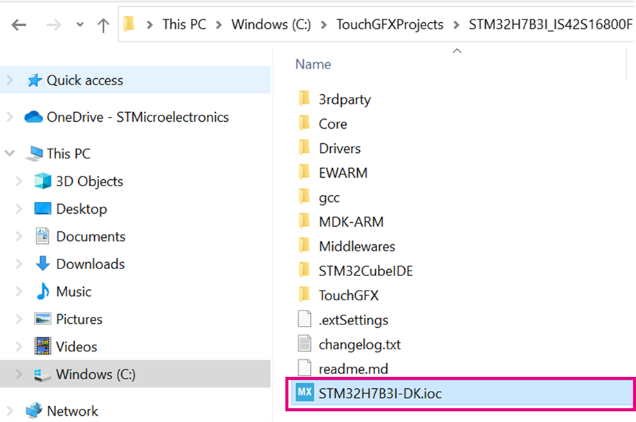
Under the project location, open the STM32CubeMx project by double-clicking on STM32H7B3I-DK.ioc
4. Set up the OSPI clock
From the OSPI memory datasheet, we see that the max clock of the OSPI is 133MHz.
Per the STM32H7B3LI datasheet, we see that the maximum OSPI clock depends on the mode (either Single-Data Rate (SDR) or Double-Transfer Rate (DTR)), the supply (VDD) voltage, and the load capacitance (CLoad). Table 89 and Table 90 (below) show the different values:
In this article we’ll use the OSPI kernel clock frequency, which is the clock that feeds the OSPI peripheral, at 133MHz. It is important to note the difference between OSPI kernel clock and the OSPI clock:
- The OSPI kernel clock is the clock that feeds the OSPI peripheral
- The OSPI clock is the clock you see on OSPI CLK pin and that’s the clock that feeds the OSPI memory
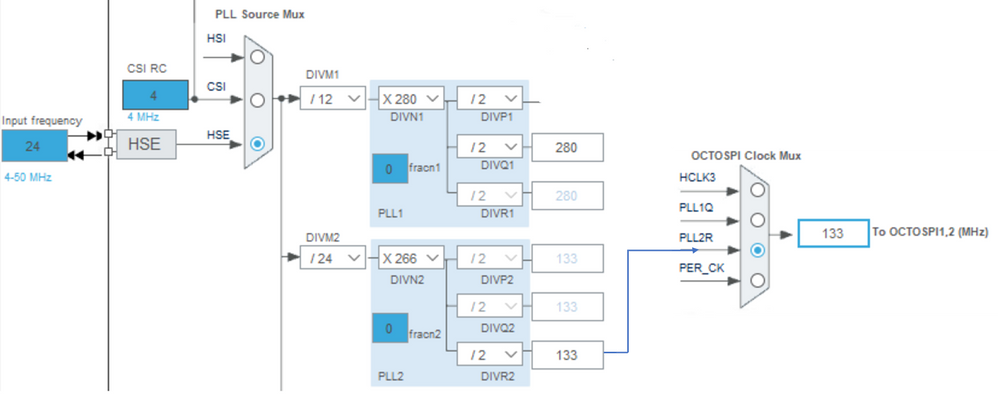
The first step is to setup the OSPI kernel clock. Here we will use PLL2 to set it to 133MHz. We’ll see later that the OSPI clock is derived from this OSPI kernel clock and using 133MHz you can get up to 133MHz as OSPI clock with the prescaler set to 1. Refer to section 6) v)
In STM32CubeMx, under the Clock Configuration Tab, we see the OCTOSPI clock mux. As shown below, the OSPI clock can be derived from PLL2, PLL1, HCLK3, or Peripheral Clock (PER_CK). Thus, we need to set up the DIVM2 and PLL2 “N” multiplier, “R” and the divider right after the output of the PLL2 in a way to get 133MHz to the OSPI peripheral.
One possible solution is to have DIVM2 = 24, N = 266, R = 2. This solution gives an OSPI kernel clock of 133MHz. This clock will get divided by 4 later in the OSPI configuration – refer to section “6) v)”.
- Set up the OSPI mode
STM32H7B3 family embeds two instances of OSPIs:
- OCTOSPI1: addressable from 0x9000 0000 in memory-mapped mode
- OCTOSPI2: addressable from 0x7000 0000 in memory-mapped mode
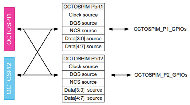
The internal pins of OSPI1 and OSPI2 each could be mapped to either port 1 or port 2 as shown below:
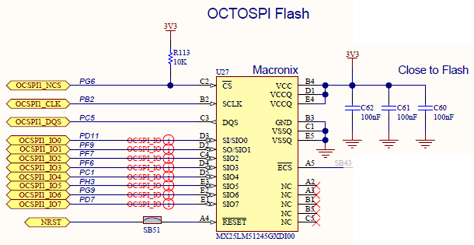
Per the schematic below:
- OCTOSPI1 is used to interface with OSPI memory.
- 8 pins for data (IO0 to IO7) meaning in the mode we need to select OCTO mode.
- DQS pin is used
 |
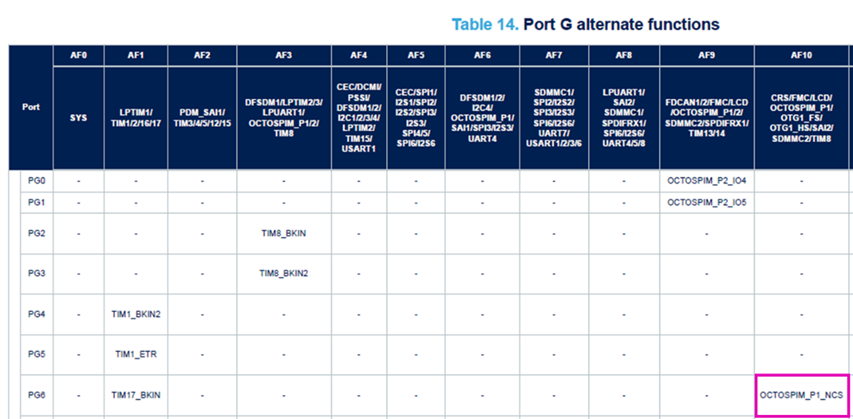
- OSPI Port 1 is selected to map the internal OSPI pins to the GPIO pins. PG6, for example, can be mapped to OCTOSPIM_P1_NCS (P1 stands for Port 1) using AF10 as shown in Table 14 of the device datasheet. Similarly, Clock, Data Strobe, Data [3:0], Data [7:4] are mapped to OSPI port 1.
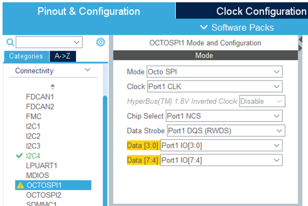
Based on the configuration above, in STM32CubeMx we can set the OSPI1 mode to OCTO mode and then use port 1 for the control and data signals.
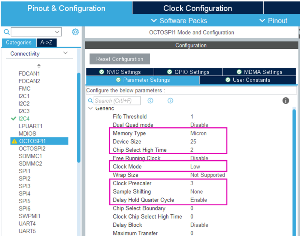
- Set the OSPI parameters
-
-
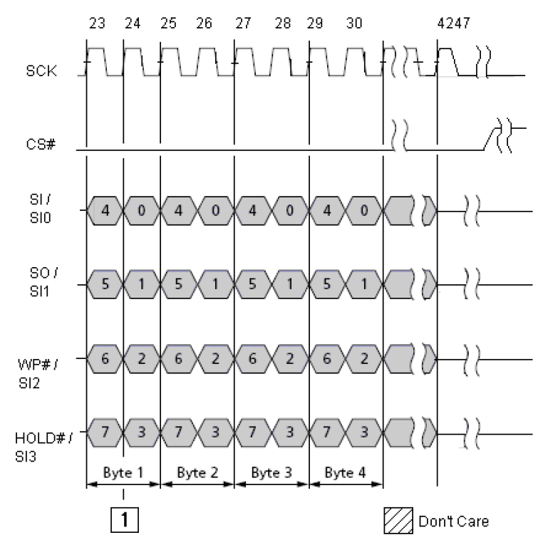
- Memory type: The data is organized D0 – D1 – D2 – D3 as shown below. In STM32CubeMx we set the mode to “Micron”:
- Memory type: The data is organized D0 – D1 – D2 – D3 as shown below. In STM32CubeMx we set the mode to “Micron”:
-
-
-
- Device Size: The size of the OSPI memory in bytes and expressed in 2^n. The datasheet of the IS25LX256 is 256MBits = 32Mbytes = 0x200 0000. We see the bit 25 is set meaning 2^25 = 32 MBytes. In STM32CubeMx we set the device size field to 25.
-
-
-
- Chip Select High Time is the minimum number of clock cycles where the CS must remain high between commands. The IS25LX256 specifies 30ns – page 88. We divide the 88ns by the clock persiod of OSPI 30ns/(133MHz / prescaler) = 133MHz / 3. The clock period is 3/133MHz. 30ns /(3/133MHz) = 1.33. we round up to the next integer value which is 2. In CubeMx we set the chip select high time to 2.
- Chip Select High Time is the minimum number of clock cycles where the CS must remain high between commands. The IS25LX256 specifies 30ns – page 88. We divide the 88ns by the clock persiod of OSPI 30ns/(133MHz / prescaler) = 133MHz / 3. The clock period is 3/133MHz. 30ns /(3/133MHz) = 1.33. we round up to the next integer value which is 2. In CubeMx we set the chip select high time to 2.
-
-
-
- The clock mode specifies the level of the clock – In page 47 of IS25LX256 datasheet, we see the memory supports Mode 0 or low level and Mode 3 which is high level. The memory supports high and low. In STM32CubeMx, we’ll select low.
- The clock mode specifies the level of the clock – In page 47 of IS25LX256 datasheet, we see the memory supports Mode 0 or low level and Mode 3 which is high level. The memory supports high and low. In STM32CubeMx, we’ll select low.
-
-
-
- Clock prescaler: In STM32CubeMx, we’ll set the prescaler to 3. This means the clock on the bus is 133MHz / 3 = 44.3MHz.
- Per the OSPI specification in RM0455, the sample shifting needs to be set to none in DTR mode – see excerpt below. In STM32CubeMx, we set sample shifting to “none”.
- Per the OSPI specification in RM0455, it is recommended to enable the delay hold quarter cycle meaning a quarter cycle delay on the outputs in DTR communication. See excerpt below from RM0455.
- The other parameters will be left with the default values.
-
- Setup the GPIO
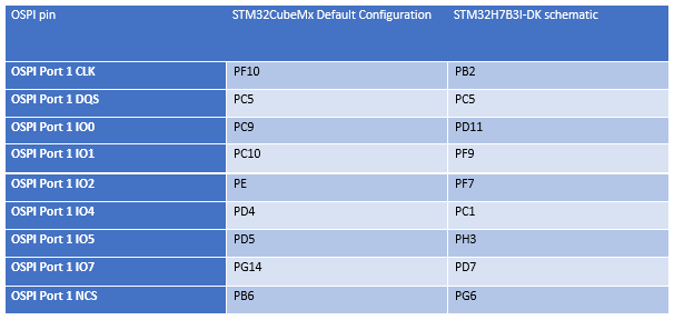
Hence, we need to change the mapping of OSPI pins listed in the table above to match the STM32H7B3I-DK schematic:
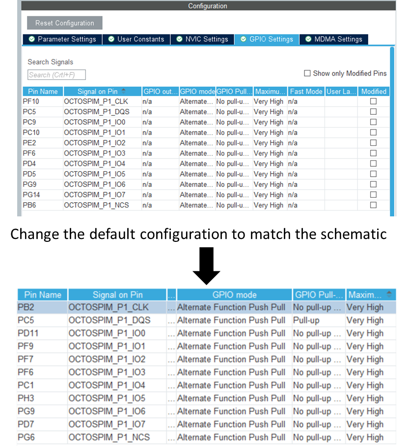
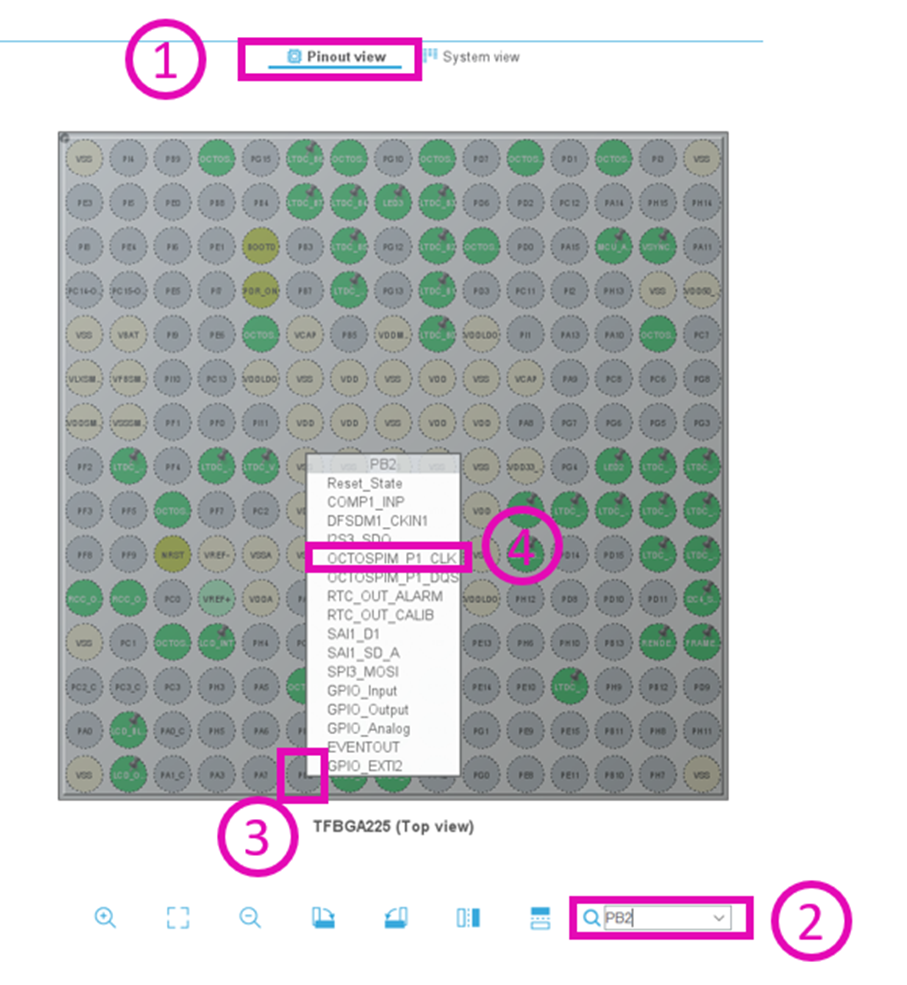
In the pinout view tab, type the name of the pin in the search field, the pin will be highlighted, left click on the pin and then change the alternate function to OSPI signal.
The example below shows how to change OSPI Port 1 CLK from PF10 to PB2:
- OSPI Configuration sequence
By default, the IS25LX256 uses 1-line SDR SPI mode with a limited maximum clock frequency. To benefit from OCTO and DTR modes at high-speed accesses we need to send specific commands as follows:
- Step 1: Reset the memory to make sure to start from the default state of the memory.
- Step 2: Setup the dummy cycles: The dummy cycles are used to give the OSPI memory the time to prepare the data with high-speed accesses. The IS25LX256 datasheet shows the dummy cycles need to be set to 5 cycles when the clock frequency is 50MHz.
- Step 3: Setup the octal DTR mode: By default, the IS25LX256 uses 1-line SDR SPI mode and to benefit from OCTO and DTR modes we need to enable them.
- Step 4: Enable the memory mapped mode. This is a configuration of the OSPI peripheral that configures the external OSPI flash memory in the internal memory space mapped at address 0x9000 0000.
The snippet code below shows the implementation of the configuration sequence:
/* USER CODE BEGIN OCTOSPI1_Init 2 */
  /* Step 1: Reset the OSPI memory */
  if(OSPI_ResetMemory(&hospi1) != 0)
  {
    Error_Handler();
  }
  /* Step 2: Setup the dummy cycles */
  if(OSPI_SetupDummyCycles(&hospi1) != 0)
  {
    Error_Handler();
  }
  if(OSPI_SetupOctalDDRMode(&hospi1) != 0)
  {
    Error_Handler();
  }
  /* Step 4: Enable the memory mapped mode */
  if(OSPI_EnableMemoryMappedMode(&hospi1) != 0)
  {
    Error_Handler();
  }
  /* USER CODE END OCTOSPI1_Init 2 */
Related links
- Mark as Read
- Mark as New
- Bookmark
- Permalink
- Email to a Friend
- Report Inappropriate Content
Hi @Laura C. ,
Thanks for the sharing.
I noticed you configured memory type to Micron in the OSPI parameter setting even though a ISSI flash was used.
I am curious to know which memory type should be selected when connecting a flash which is not in the supported list?
The supported list I refered to is stm32xxx_hal_ospi.h.
#define IS_OSPI_MEMORY_TYPE(TYPE)
                                            (((TYPE) == HAL_OSPI_MEMTYPE_MICRON)      || \
                                            ((TYPE) == HAL_OSPI_MEMTYPE_MACRONIX)     || \
                                            ((TYPE) == HAL_OSPI_MEMTYPE_APMEMORY)     || \
                                            ((TYPE) == HAL_OSPI_MEMTYPE_MACRONIX_RAM) || \
                                            ((TYPE) == HAL_OSPI_MEMTYPE_HYPERBUS))
I am currently working on STM32U575 so the file name is stm32u5xx_hal_ospi.h.
- Mark as Read
- Mark as New
- Bookmark
- Permalink
- Email to a Friend
- Report Inappropriate Content
@Glee.4 I agree this could be confusing. The memory type depends on the D0/D1 ordering: The micron (and compatible memories) use D0/D1 Ordering while Macronix (and compatible memories) use D1/D0 data ordering.
If you have a memory different from Micron and Macronix you simply need to look at the data ordering in the memory datasheet and then select the one that matches it in STM32 OSPI configuration.
That’s what I did with ISSI memory. It is not listed so I looked at the data ordering in ISSI memory datasheet and I figured it is compatible with Micron.
I hope this helps and let me know if you have any questions.
With regards,
Badreddine
- Mark as Read
- Mark as New
- Bookmark
- Permalink
- Email to a Friend
- Report Inappropriate Content
Hi @ame MCU Support Center BB ,
My case is kind of tricky that the memory (ISSI S37SML01G1) only supports Quad SPI.
I am managing connect a QSPI memory to STM32's OSPI port.
Not sure which memory type I should select.
- Mark as Read
- Mark as New
- Bookmark
- Permalink
- Email to a Friend
- Report Inappropriate Content
@Glee.4 I think it is better to submit an online support ticket for your question.
- Mark as Read
- Mark as New
- Bookmark
- Permalink
- Email to a Friend
- Report Inappropriate Content
I am a bit confused on the arithmetic here. Referring to Application Note AN5050 Rev 8 (Getting started with Octo-SPI and Hexadeca-SPI Interface on STM32 microcontrollers):
On page 44, Table 7 specifies the value 26 (64 Mbytes) for the Octal-SP Flash Macronix MX25LM51245.
However, that row also includes Note(3) for device sizes which says:
3. Device size (DEVSIZE) defines the memory size in number of bytes = 2^(DEVSIZE+1).
If I use the formula in Note 3 then setting the value of DEVSIZE fo 26 results in 128MBytes of memory.
What is going on here?
- Mark as Read
- Mark as New
- Bookmark
- Permalink
- Email to a Friend
- Report Inappropriate Content
The formula is consistent with the hardware expectations. 2**27=128MByte DEVSIZE=26
If DEVSIZE = 31 (5-bit register) is basically an infinitely size device.
Being too big is NOT a serious problem, it will just appear that the device wraps within the address space. If it is too small on the other hand, the MCU will Hard Fault when you hit the lower memory limit for the decoding logic.
- Mark as Read
- Mark as New
- Bookmark
- Permalink
- Email to a Friend
- Report Inappropriate Content
In other words, the value of 26 (for the device size) in the Application Note AN5050 is 'wrong' and needs to be corrected. Otherwise people like me will be scratching their heads trying to determine who/what/when to believe.
- Mark as Read
- Mark as New
- Bookmark
- Permalink
- Email to a Friend
- Report Inappropriate Content
Well, the Reference Manual is typically the Controlling Document here. If things are confusing or inconsistent, weight your understanding against what's in the RM as to the register level function. Look also at the library source, this can often be a source of off-by-one issues where the stuff in the structure isn't exactly what's in the register, and this may also change from platform-to-platform.
The trick here is to touch all your memory locations when confirming if it works, or not.
Watch out also for errata, there are some F7/H7 issues with reading the last 32-bytes of QSPI
@AME MCU Support Center BB @Amel NASRI please flag the AN5050 for review
- Mark as Read
- Mark as New
- Bookmark
- Permalink
- Email to a Friend
- Report Inappropriate Content
Hi @Tesla DeLorean ,
Thanks for keeping me in the loop, we will take care to align AN5050 and the reference manuals.
-Amel
- Mark as Read
- Mark as New
- Bookmark
- Permalink
- Email to a Friend
- Report Inappropriate Content
can you provide source for the OSPI_SetupOctalDDRMode function? The ISSI device is different from the Macronix device in the specifics of how to configure Octal DDR mode so a known-good example of the command would be useful.
- Mark as Read
- Mark as New
- Bookmark
- Permalink
- Email to a Friend
- Report Inappropriate Content
I'd imagine you'd have some existing patterns you can verify, and try a couple of commands and setting permutations based on a review of the data sheets, and see if some magic happens.
- Mark as Read
- Mark as New
- Bookmark
- Permalink
- Email to a Friend
- Report Inappropriate Content
hi @AME MCU Support Center BB @Amel NASRI
this is very generic description
I have seen a few youtube presentations by STM32 team, they explain how OSPI works
but without some basic sample code for a start to read maybe registers of the OSPI to see that something is working
that kind of presentation is useless.
it leaves you with days or weeks trying to find out the right code to read and write.
I tried some of the example codes from CubeMX to use on my custom board. Nothing seems to be working.
QSPI seems easier to implement a lot of material on youtube I have a few boards working with QSPI.
