- STMicroelectronics Community
- Knowledge base
- STM32 MCUs
- How to set up the FMC peripheral to interface with...
- Subscribe to RSS Feed
- Mark as New
- Mark as Read
- Bookmark
- Subscribe
- Email to a Friend
- Printer Friendly Page
- Report Inappropriate Content
How to set up the FMC peripheral to interface with the SDRAM IS42S16800F-6BLI from ISSI
- Subscribe to RSS Feed
- Mark as New
- Mark as Read
- Bookmark
- Subscribe
- Email to a Friend
- Printer Friendly Page
- Report Inappropriate Content
on 2021-12-21 2:27 AM - edited on 2024-06-12 3:32 AM by FBL
Introduction
It is very common for HMI-of-Things applications to have the capability to control and display data between a user and the machine. Such applications require the ability to interface with external memory such as SDRAM that is used as frame (or video) buffer and as a cache for the graphics assets. The STM32’s integrated Flexible Memory Controller (FMC) peripheral makes it easy to interface with external memories.
In this article we will see how to configure the FMC peripheral of the STM32 to interface with the SDRAM IS42S16800F-6BLI from ISSI – datasheet available via the link below:
https://www.issi.com/WW/pdf/42-45S81600F-16800F.pdf
The SDRAM is available for mass market from Digi-Key:
https://www.digikey.com/en/products/detail/issi-integrated-silicon-solution-inc/IS42S16800F-6BLI/4860927
1. Prerequisites
1.1 Hardware
- STM32H7B3LI
1.2 Software
- TouchGFX Designer
- STM32CubeIDE
- STM32CubeMx
In this article we’ll see how to set up the FMC peripheral in the STM32H7B3I-DK TouchGFX Board Setup (TBS) to have the ability to have the frame buffers in the SDRAM IS42S16800F-6BLI.
2. Steps
2.1 Create a TouchGFX application
Create a TouchGFX application based on the STM32H7B3I-DK Board Setup. If you don’t know how to do this step, please refer to this link: https://support.touchgfx.com/4.18/docs/tutorials/tutorial-02. The tutorial uses the STM32F746G-DK while in this article we’ll be using the STM32H7B3I-DK.
2.1 Open the STM32CubeMx project
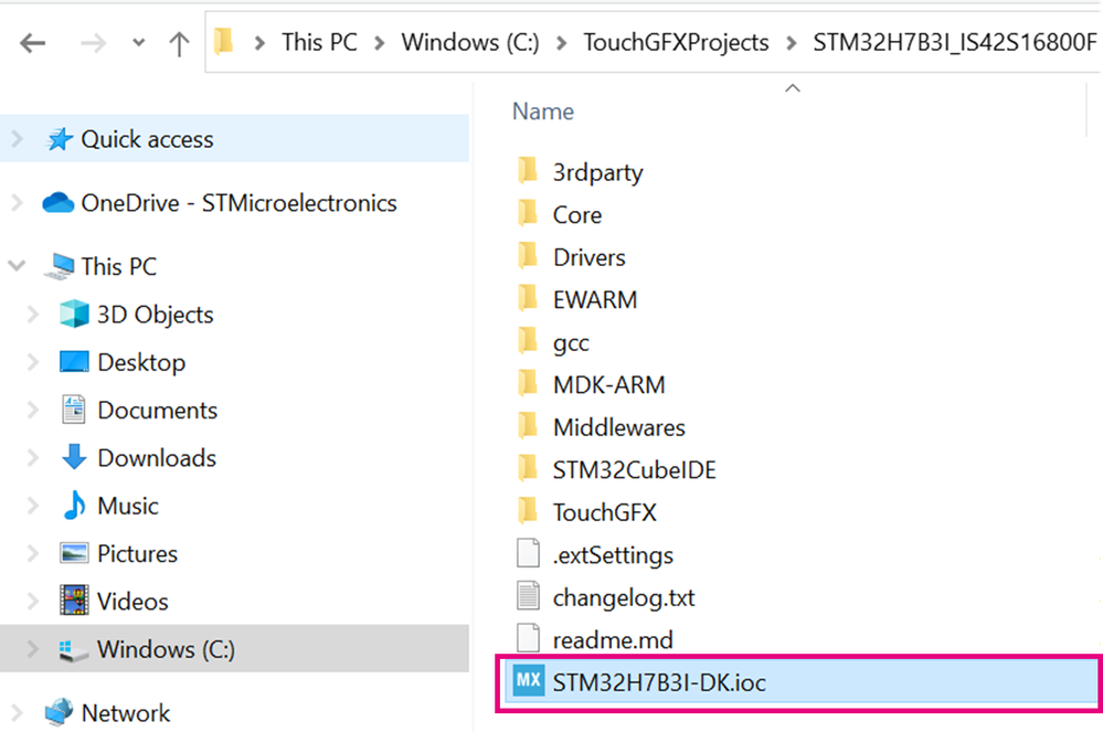
Under the project location, open the STM32CubeMx project by double-clicking on STM32H7B3I-DK.ioc
 |
2.2 Set up the FMC clock
When we look at the SDRAM datasheet, we see the max clock of the SDRAM depends on the Column Address Strobe CAS latency. For our SDRAM, “-6” variant, the CAS latency can be set to 2 and the max clock frequency would be 100MHz and could be set to 3 clock cycles and the max clock frequency would be 166MHz.
 |
On the other side, when we look at the STM32H7B3LI datasheet, we see the maximum FMC clock at VDD = 3.3V is 110MHz.
 |
In this article we’ll use the FMC clock frequency (which is the clock that will feed the SDRAM) at 100MHz and the CAS latency to 2.
The first step is to setup the clock to the FMC peripheral. Here we will use PLL2 to set it to 200MHz. We’ll see later that the SDRAM clock is derived from this FMC clock and using 200MHz you can get up to 100MHz as clock frequency for the SDRAM with the divider set to 2.
In STM32CubeMx, under the Clock Configuration Tab, we see the FMC clock mux. As shown below, the FMC clock is derived from PLL2. Thus, we need to set up the DIVM2 and PLL2 “N” multiplier, “R” and the divider right after the output of the PLL2 in a way to get 200MHz to the FMC.
One possible solution is to have DIVM2 = 24, N = 200, R = 1. This solution gives an FMC clock of 200MHz. This clock will get divided by 2 later in the FMC – ref. “SDRAM common clock”
2.3 Set up the SDRAM
The SDRAM IS42S16800F-6BLI has the following main features:
- 4096 rows by 512 columns
- 4 banks
- 12-bit address: A0…A11
- 16-bit data: D0…D15
- Self-refresh time = 64ms
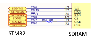
The FMC can support up to two SDRAM banks: SDRAM1 and SDRAM2 256Mbit each. SDRAM1 is mapped at the address 0xC000 0000 and SDRAM2 is mapped at address 0xD000 0000. The SDRAM on the STM32H7B3I-DK Discovery Kit is connected to the SDRAM2 interface. As you can see in the schematic below, the SDCKE1 signal is connected to the SDRAM clock input and SDNE1 is connected to the chip select/enable input.
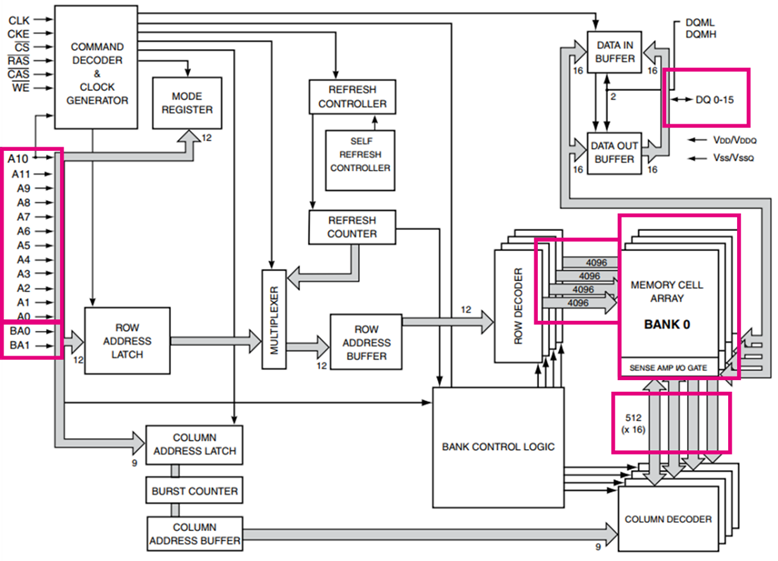
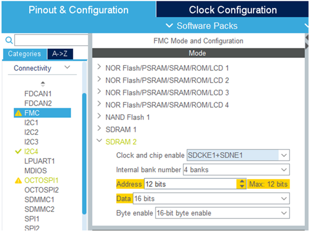
As shown above by the block diagram of the SDRAM IS42S16800F-6BLI, the memory has 4 banks, 12 bits of address, 16 bits of data and 16-bit byte enable. All we need to do is to provision the SDRAM characteristics as shown below:
The next step is to setup the following parameters:
- Number of columns: we need 9 bits to code the 512 columns. In STM32CubeMx, we need to set the number of column address bits to 9 bits.
- Number of rows: we need 12 bits to code the 4096 rows. In STM32CubeMx, we need to set the number of row address bits to 12 bits.
- CAS Latency: The CAS latency is 2 at 100MHz. In STM32CubeMx, we set the CAS latency to 2.
- Write protection: We will disable the write protection.
- SDRAM clock: The SDRAM maximum clock frequency is 100MHz at CAS latency of 2. In STM32CubeMx we set the divider to 2. This gets us an SDRAM clock of FMC clock divided by 2 meaning 200MHz/2=100MHz.
- We’ll enable the burst read for single read request and set the pipe delay to 2 clock cycles.
 2.4 Setup the SDRAM timings
The datasheet of the SDRAM IS42S16800F-6BLI specifies a set of timing values in which some of them need to be provisioned in STM32CubeMx such as tRC, tRAS,….:
- We’ll start with the load mode register to active delay (tMRD) which indicates the delay between the load mode register command and the row or refresh command. The memory datasheet specifies 12ns which needs to be converted to a number of memory cycles. So, we divide the 12ns by the SDRAM clock period which is 10ns and then we round to the upper value and is the value we use in STM32CubeMx.
- Second, the exit self-refresh delay (tXSR)is the Exit self-refresh to delay between valid commands. The memory datasheet specifies 67ns and is converted to 7 SDRAM clock cycles and is the value we use in STM32CubeMx.
- Third, the self-refresh time defined (tRAS) is the Delay between line valid and precharge command. The memory datasheet specifies 42ns and is converted to 5 SDRAM clock cycles and is the value we use in STM32CubeMx.
- After that, the common row cycle delay (tRC) is the Delay between two refresh commands or two lines of valid commands. The memory datasheet specifies 60ns and and is converted to 6 SDRAM clock cycles and is the value we use in STM32CubeMx.
- Next, the write recovery time (tDPL) is the Delay between writing a command to a precharge command. The memory datasheet specifies 12ns and when we convert it to SDRAM clock cycles we get 2 while the specification of the STM32 requires having TWR >= TRAS – TRCD=5-2=3 and that’s the value we use in STM32CubeMx.
- After that, the common row precharge delay (tRP) is the Delay between precharge and line valid commands. The memory datasheet specifies 18ns and when converted is 2 SDRAM clock cycles and that’s the value we use in STM32CubeMx.
- The Last parameter is the row to column delay (tRCD) and indicates the delay between the line valid command and the read/write command. The memory datasheet specifies 18ns and is converted to 2 SDRAM clock cycles and that’s the value we use in STM32CubeMx.

2.5 Setup the GPIO
Finally, we select Under GPIO settings Tab, we see that the STM32CubeMx default pinout for SDRAM matches the STM32H7B3I-DK schematic except for the following pins: FMC_SDCKE1SDCKE1, FMC_SDNE1, and FMC_SDNWE
- STM32CubeMx selects PB5 for SD clock enable 1 by default while the schematic uses PH7
- STM32CubeMx selects PB6 for SD chip enable by default while the schematic uses PH6
- STM32CubeMx selects PC0 for SD write enable by default while the schematic uses PH5
Hence, we need to change the mapping of FMC_SDCKE1, FMC_SDNE1 and FMC_SDNWE to match the STM32H7B3I-DK schematic.

In the pinout view tab, type the name of the pin in the search field, the pin will be highlighted, left click on the pin and change the alternate function to SDRAM signal. The example below shows how to change FMC_SDCEK1 to PH7.
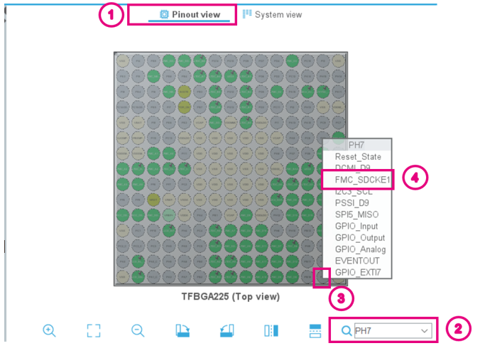
2.6 SDRAM Initialization sequence
The STM32 can’t start reading and writing data immediately from/to the SDRAM after power-on. The SDRAM requires an initialization sequence to be accessible. The initialization sequence as described in section 23.9.3 SDRAM controller functional description in the reference manual RM0455 is:
Step 1 and Step 2: Setup the SDRAM timing and was done in the previous steps using STM32CubeMx section 4 and section 5
Step 3: Issue a clock enable command
Step 4: Wait for a min of 100us
Step 5: Configure the precharge all command
Step 6: Issue the Auto refresh command
Step 7: Program the external memory mode
Step 8: Setup the refresh counter using the formula refresh time divided number of rows times the SDRAM clock and then minus 20 and this gives us 1542
The initialization sequence step 3 to step 7 is not generated by STM32CubeMx – It is up to the user add it manually.
The snippet code below shows the implementation of the initialization sequence:
 /* USER CODE BEGIN FMC_Init 2 */
  FMC_SDRAM_CommandTypeDef Command;
  /* Step 1 and Step 2 already done in HAL_SDRAM_Init() */
  /* Step 3: Configure a clock configuration enable command */
   Command.CommandMode            = FMC_SDRAM_CMD_CLK_ENABLE; /* Set MODE bits to "001" */
   Command.CommandTarget          = FMC_SDRAM_CMD_TARGET_BANK2; /* configure the Target Bank bits */
   Command.AutoRefreshNumber      = 1;
   Command.ModeRegisterDefinition = 0;
   HAL_SDRAM_SendCommand(&hsdram2, &Command, 0xfff);
   HAL_Delay(1); /* Step 4: Insert 100 us minimum delay - Min HAL Delay is 1ms */
   /* Step 5: Configure a PALL (precharge all) command */
   Command.CommandMode            = FMC_SDRAM_CMD_PALL; /* Set MODE bits to "010" */
   HAL_SDRAM_SendCommand(&hsdram2, &Command, 0xfff);
   /* Step 6: Configure an Auto Refresh command */
   Command.CommandMode            = FMC_SDRAM_CMD_AUTOREFRESH_MODE; /* Set MODE bits to "011" */
   Command.AutoRefreshNumber      = 2;
   HAL_SDRAM_SendCommand(&hsdram2, &Command, 0xfff);
   /* Step 7: Program the external memory mode register */
   Command.CommandMode            = FMC_SDRAM_CMD_LOAD_MODE;/*set the MODE bits to "100" */
   Command.ModeRegisterDefinition =  (uint32_t)0 | 0<<3 | 2<<4 | 0<<7 | 1<<9;
   HAL_SDRAM_SendCommand(&hsdram2, &Command, 0xfff);
   /* Step 8: Set the refresh rate counter - refer to section SDRAM refresh timer register in RM0455 */
   /* Set the device refresh rate
    * COUNT = [(SDRAM self refresh time / number of row) x  SDRAM CLK] – 20
            = [(64ms/4096) * 100MHz] - 20 = 1562.5 - 20 ~ 1542 */
   HAL_SDRAM_ProgramRefreshRate(&hsdram2, 1542);
  /* USER CODE END FMC_Init 2 */
Related links
STM32H7B3LI – Datasheet
STM32H7A3/7B3 and STM32H7B0 Value line advanced Arm<Sup>®</Sup>-based 32-bit MCUs - Reference manual
STM32CubeMx - STM32Cube initialization code generator
STM32H7B3I-DK - Discovery kit with STM32H7B3LI MCU
TouchGFX Documentation
- Mark as Read
- Mark as New
- Bookmark
- Permalink
- Email to a Friend
- Report Inappropriate Content
Very helpful and detailed article. Thank you!
- Mark as Read
- Mark as New
- Bookmark
- Permalink
- Email to a Friend
- Report Inappropriate Content
STM32H750IBK6 REV V sample what is max FMC CLK we can run SDRAM
datasheet says 2 value for rev V and REV Y
- Mark as Read
- Mark as New
- Bookmark
- Permalink
- Email to a Friend
- Report Inappropriate Content
Thank you for explaining the complicated topic and braking it down to the necessery timing parameters. Very helpful!
- Mark as Read
- Mark as New
- Bookmark
- Permalink
- Email to a Friend
- Report Inappropriate Content
Extremely useful (I would daresay essential) guide for setting up SDRAM. Two observations/suggestions:
1) Reading the datasheet for the FMC in the STM32H743, it is not at all obvious that FMC_CLK / 2 = SDRAM_CLK. I mean, based on experience with other MCUs I suspected it was, and the "SDRAM common clock" setting should also suggest that, but it would be super-handy if in CubeMX you displayed the effective SDRAM clock speed somewhere in the configuration box.
2) Specifying which named timing parameter (e.g. t-DPL) corresponds to which configuration option is invaluable. It would be EXTREMELY helpful if these timing parameter names were included in the help info text, if not in the name of the parameter itself.
Dana M.
- Mark as Read
- Mark as New
- Bookmark
- Permalink
- Email to a Friend
- Report Inappropriate Content
Thank you for this helpful article. However with STM32CubeMX Version 6.10.0 and 6.11.1 I get an error (FMC Clock Source frequency must be =< 133 Mhz) when FMC Clock Source is configured to be 200 MHz which was allowed in previous versions of CubeMX.

Is this a bug in CubeMX?
- Mark as Read
- Mark as New
- Bookmark
- Permalink
- Email to a Friend
- Report Inappropriate Content
@bbee You may be better off creating a new topic, I'm not sure that ST will reply here. However, I'm unable to reproduce your issue. I'm using the latest IDE (1.15.1) and the latest STM32 FW H7 (1.11.2), and the tool tells me (in my present config) that my max FMC clock is 300 MHz.

It is entirely likely that the flagged maximum value of the FMC input depends on what mode(s) you are operating the FMC in. For SDRAM mode, you can feed 300 MHz to the FMC, then the FMC will internally divide that down by up to div/3 to yield a 100 MHz memory clock. I'm guessing you've selected a memory mode or type that has different restrictions on what fmc_ker_ck frequency can be selected. If you do create a new topic on this, @ tag me, and I'll see if I can help further. (I can't attach an .ioc or .zip file here.)
Dana M.
- Mark as Read
- Mark as New
- Bookmark
- Permalink
- Email to a Friend
- Report Inappropriate Content
@dmarks-lsThank you for your response.
In the meantime I managed to figure out the reason by myself. The maximum allowed frequency for FMC depends on the selected Power Regulator Voltage Scale. In my Project I selected VOS3 for which the maximum allowed frequency is 133 Mhz. CubeMX knows it, but gives no hint related to the power parameter. I switched to VOS2 which allows a maximum of 200 Mhz.
- Mark as Read
- Mark as New
- Bookmark
- Permalink
- Email to a Friend
- Report Inappropriate Content
You should follow up with this:
Basically you need cache management and MPU configuration to have best performance of the FMC interface with STM32H7. I added this code, and calling it before the SCB_EnableICache(), SCB_EnableDCache() part:
static void MPU_ConfigSDRAM(void) {
MPU_Region_InitTypeDef MPU_InitStruct;
HAL_MPU_Disable();
MPU_InitStruct.Enable = MPU_REGION_ENABLE;
MPU_InitStruct.BaseAddress = SDRAM_ADDR_BLOCK1;
MPU_InitStruct.Size = MPU_REGION_SIZE_1MB;
MPU_InitStruct.AccessPermission = MPU_REGION_FULL_ACCESS;
MPU_InitStruct.IsBufferable = MPU_ACCESS_BUFFERABLE;
MPU_InitStruct.IsCacheable = MPU_ACCESS_CACHEABLE;
MPU_InitStruct.IsShareable = MPU_ACCESS_NOT_SHAREABLE;
MPU_InitStruct.Number = MPU_REGION_NUMBER0;
MPU_InitStruct.TypeExtField = MPU_TEX_LEVEL1;
MPU_InitStruct.SubRegionDisable = 0x00;
MPU_InitStruct.DisableExec = MPU_INSTRUCTION_ACCESS_DISABLE;
HAL_MPU_ConfigRegion(&MPU_InitStruct);
HAL_MPU_Enable(MPU_PRIVILEGED_DEFAULT);
}
- Mark as Read
- Mark as New
- Bookmark
- Permalink
- Email to a Friend
- Report Inappropriate Content
Hey,
Could you please explain what the "read pipe delay" is and why its set to "2 HCLK clock cycles"
I found this is from the STM32H747 reference manual.
It says the FIFO is used to store data read in advance during the CAS latency period. But during the latency period we wait for data from the device (right?).
And how does the RPIPE (read pipe delay) change how much data is held in the FIFO (from the examples).
Thank you

