- STMicroelectronics Community
- Knowledge base
- STM32 MCUs
- DMA is not working on STM32H7 devices
- Subscribe to RSS Feed
- Mark as New
- Mark as Read
- Bookmark
- Subscribe
- Email to a Friend
- Printer Friendly Page
- Report Inappropriate Content
DMA is not working on STM32H7 devices
- Subscribe to RSS Feed
- Mark as New
- Mark as Read
- Bookmark
- Subscribe
- Email to a Friend
- Printer Friendly Page
- Report Inappropriate Content
on
2018-07-23
06:21 AM
- edited on
2024-06-04
04:47 AM
by
![]() Laurids_PETERSE
Laurids_PETERSE
The problem is related to two things: memory layout on STM32H7 and internal data cache (D-Cache) of the Cortex-M7 core.
In summary these can be the possible issues:
- Memory placed in DTCM RAM for D1/D2 peripherals. Unfortunately this memory is used as default in some projects including examples.
- Memory not placed in D3 SRAM4 for D3 peripherals.
- D-Cache enabled for DMA buffers, different content in cache and in SRAM memory.
- Starting the DMA just after writing the data to TX buffer, without placing __DSB() instruction between.
For Ethernet related problems, please see separate FAQ: FAQ: Ethernet not working on STM32H7x3
1. Explanation: Memory layout
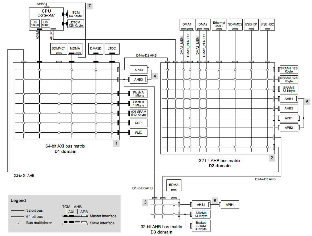
The STM32H7 device consists of three bus matrix domains (D1, D2 and D3) as seen on the picture below. The D1 and D2 are connected through bus bridges, both can also access data in D3 domain. However there is no connection from D3 domain to D1 or D2 domain.
The DMA1 and DMA2 controllers are located in D2 domain and can access almost all memories with exception of ITCM and DTCM RAM (located at 0x20000000). This DMA is used in most cases.
BDMA controller is located in D3 domain and can access only SRAM4 and backup SRAM in the D3 domain.
MDMA controller is located in D1 domain and can access all memories, including ITCM/DTCM. This controller is mainly used for handling D1 peripherals and memory to memory transfers.
From performance point of view it is better to put DMA buffers inside D2 domain (SRAM1, SRAM2 and SRAM3), since the D2-to-D1 bridge can add additional delay.
2. Explanation: Handling DMA buffers with D-Cache enabled
The Cortex-M7 contains two internal caches, I-Cache for loading instructions and D-Cache for data. The D-Cache can affect the functionality of DMA transfers, since it will hold the new data in the internal cache and don't write them to the SRAM memory. However the DMA controller loads the data from SRAM memory and not D-Cache.
In case the DMA transfer is started just after writing the data to the tx_buffer in the code, it can happen that the tx_buffer data will be still in write-buffer inside the CPU, while the DMA is already started. Solution can be to set the tx_buffer as device type and force CPU to order the memory operations, or add __DSB() instruction before starting the DMA.
There are several ways how to keep manage DMA buffers with D-Cache:
- Disable D-Cache globally. It is the most simple solution, but not effective one, since you can loose great part of performance. Can be useful for debugging, to analyze if the problem is related to D-Cache.
- Disable D-Cache for part of the memory. This can be done by configuring the memory protection unit (MPU). The downside is that the MPU regions have certain alignment restrictions and you need to place the DMA buffers to specific parts of memory. Each toolchain (GCC, IAR, KEIL) needs to be configured in different way.
- Note that MPU regions can overlap and the higher region number has priority. Together with subregion disable bits, this can be useful to soften the alignment and size restrictions.
- Note that Device and Strongly ordered memory types not allow unaligned access to the memory.
- Configure part of memory as write-through. Can be used only for TX DMA. Similar to the previous option.
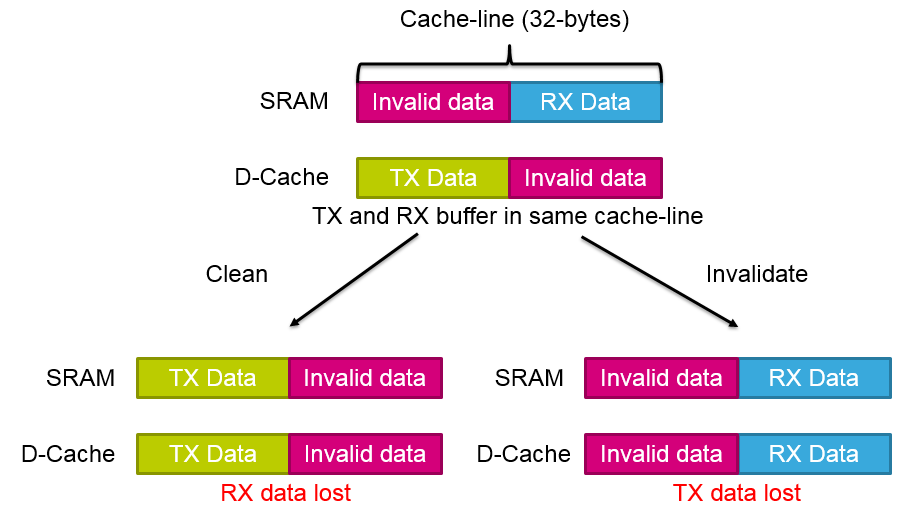
- Use cache maintenance operations. It is possible to write data stored in cache back to memory ("clean" operation) for specific address range, and also discard data stored in cache ("invalidate" operation).
- The downside is that these operations work withe cache-line size which is 32 bytes, so you can't clean or invalidate single byte from the cache. This can lead to errors when RX buffer "shares" the cache line with other data or TX buffer (please see the picture below).
- Beware that with uninitialized D-Cache, the maintenance operations "clean" or "clean and invalidate" can lead to BusFault exception. This is caused by uninitialized ECC (error correction code) after power-on reset. If you have project with a lot of maintenance operations and want to disable D-Cache temporarily, you can use SCB_InvalidateDCache function, which will clean the cache and set correct ECC, without enabling it.
Below are the possible MPU configurations. Green are configurations suitable for DMA buffers, blue is suitable only for TX-only DMA buffer and red are forbidden. Other configurations are not suitable for DMA buffers and will require cache maintenance operations:
3. Solution example 1: Simple placement of all memory to D1 domain
D-Cache must be disabled globally for this solution to work.
GCC (Atollic TrueStudio/System Workbench for STM32/Eclipse)
Replace DTCMRAM with RAM_D1 for section placement in linkerscript (.ld file extension). E.g. like this:
.data :
{
  ... /* Keep same */
} >RAM_D1 AT> FLASH
This should be done also for .bss and ._user_heap_stack sections.
In some linkerscripts, the initial stack is defined separately. So you either need to update it with the section, or define it inside the section like:
._user_heap_stack :
{
 . = ALIGN(8);
 PROVIDE ( end = . );
 PROVIDE ( _end = . );
 . = . + _Min_Heap_Size;
 . = . + _Min_Stack_Size;
 _estack = .; /* <<<< line added */
 . = ALIGN(8);
} >RAM_D1
And remove the original _estack definition.
IAR (in project settings):
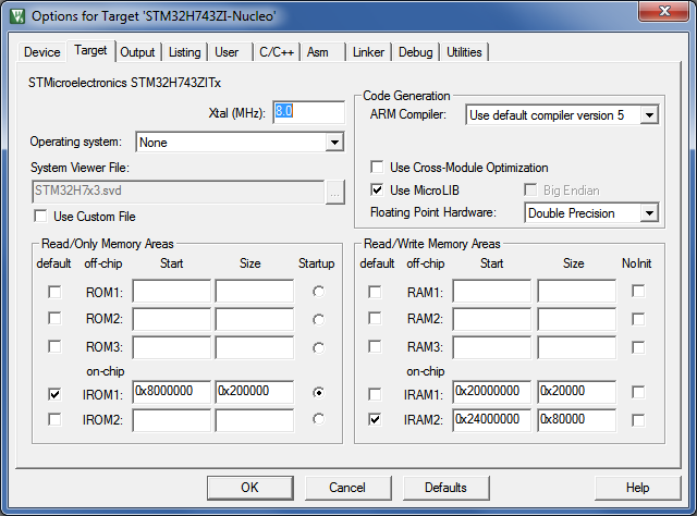
For Keil:
4. Solution example 2: Placing buffers in separated memory part
D-Cache must be disabled via MPU for that particular memory region, where DMA buffer is placed. Please note that MPU region size must be in power of two. Also the regions start address must have same alignment as size. E.g. if the regions is 512 bytes, the start address must be aligned to 512 bytes (9 LSBs must be zero).
NOTE: IAR compiler and Keil compiler version <= 5 allow placing variables at absolute address in code using compiler specific extensions.
C code:
Define placement macro:
#if defined( __ICCARM__ )
  #define DMA_BUFFER \
      _Pragma("location=\".dma_buffer\"")
#else
  #define DMA_BUFFER \
      __attribute__((section(".dma_buffer")))
#endif
Specify DMA buffers in code:
DMA_BUFFER uint8_t rx_buffer[256];GCC linkerscript (*.ld file)
Place section to D2 RAM (you can also specify your own memory regions in linkerscript file):
.dma_buffer : /* Space before ':' is critical */
{
  *(.dma_buffer)
} >RAM_D2
This is without default value initialization. Otherwise you need to place special symbols and add your own initialization code.
IAR linker file (*.icf file)
define region D2_SRAM2_region   = mem:[from 0x30020000 to 0x3003FFFF];
place in D2_SRAM2_region { section .dma_buffer};
initialize by copy { section .dma_buffer}; /* optional initialization of default values */
Keil scatter file (*.sct file)
LR_IROM1 0x08000000 0x00200000  {    ; load region size_region
  ER_IROM1 0x08000000 0x00200000  {  ; load address = execution address
   *.o (RESET, +First)
   *(InRoot$$Sections)
   .ANY (+RO)
  }
  RW_IRAM2 0x24000000 0x00080000  {  ; RW data
   .ANY (+RW +ZI)
  }
  ; Added new region
  DMA_BUFFER 0x30040000 0x200 {
  *(.dma_buffer)
  }
}
Generation of scatter file should be disabled in Keil:
5. Solution example 3: Use Cache maintenance functions
Transmitting data:
#define TX_LENGTH  (16)
uint8_t tx_buffer[TX_LENGTH];

/* Write data */
tx_buffer[0] = 0x0;
tx_buffer[1] = 0x1;

/* Clean D-cache */
/* Make sure the address is 32-byte aligned and add 32-bytes to length, in case it overlaps cacheline */
SCB_CleanDCache_by_Addr((uint32_t*)(((uint32_t)tx_buffer) & ~(uint32_t)0x1F), TX_LENGTH+32);

/* Start DMA transfer */
HAL_UART_Transmit_DMA(&huart1, tx_buffer, TX_LENGTH);
Receiving data:
#define RX_LENGTH  (16)
uint8_t rx_buffer[RX_LENGTH];

/* Invalidate D-cache before reception */
/* Make sure the address is 32-byte aligned and add 32-bytes to length, in case it overlaps cacheline */
SCB_InvalidateDCache_by_Addr((uint32_t*)(((uint32_t)rx_buffer) & ~(uint32_t)0x1F), RX_LENGTH+32);

/* Start DMA transfer */
HAL_UART_Receive_DMA(&huart1, rx_buffer, RX_LENGTH);/* No access to rx_buffer should be made before DMA transfer is completed */Please note that in case of reception there can be problem if rx_buffer is not aligned to the size of cache-line (32-bytes), because during the invalidate operation another data sharing the same cache-line(s) with rx_buffer can be lost.
6. References
- "AN4838: Managing memory protection unit (MPU) in STM32 MCUs"
- "AN4839: Level 1 cache on STM32F7 Series and STM32H7 Series":
- "AN4296: Overview and tips for using STM32F303/328/334/358xx CCM RAM with IAR EWARM, Keil MDK-ARM and GNU-based toolchains":
- "AN4891: STM32H7x3 system architecture and performance software expansion for STM32Cube":
- Mark as Read
- Mark as New
- Bookmark
- Permalink
- Email to a Friend
- Report Inappropriate Content
Seems as though the latest generated versions of the .ld files in cube fix this issue.
- Mark as Read
- Mark as New
- Bookmark
- Permalink
- Email to a Friend
- Report Inappropriate Content
It would be nice if this article would be adapted also for 'F7.
JW
- Mark as Read
- Mark as New
- Bookmark
- Permalink
- Email to a Friend
- Report Inappropriate Content
Thank you for article.
Some comments:
- Mark as Read
- Mark as New
- Bookmark
- Permalink
- Email to a Friend
- Report Inappropriate Content
I seem to have this issue on STM32H7A3, while using ADC1 with DMA1. ADC keep running into overriding error, and searches led me to here. However, it seems that my .ld script is configured a little different, I only found RAM_EXEC used and not DTCMRAM (Tried solution 1). Also, SCB_DisableDCache(); leads to hardfault. I probably don't know what I'm doing, as until now I haven't run into need for modifying memory, so a little more detailed guidance would be appreciated. Thank you.
- Mark as Read
- Mark as New
- Bookmark
- Permalink
- Email to a Friend
- Report Inappropriate Content
@Adam BERLINGER , please, can you help?
- Mark as Read
- Mark as New
- Bookmark
- Permalink
- Email to a Friend
- Report Inappropriate Content
Hi!
I have read your article in past and try to dissable D-cache in Keil scatter file - it did not help for me.
Here is my problem https://community.st.com/s/question/0D53W00001atD9zSAE/stm32h7-spi-dma-not-working
I have STM32H745 nucleo. I want to use M4 core . In D2 domain i use SRAM1-SRAM3, DMA2 . I need to send data via SPI-DMA (SPI4, PE14 MOSI, DMA2_stream3, DMAUX11 ) I dont have any on MOSI pin + DMA2_IRQ_Handler don't work.
The same i have corectly did on stm32f407 - all worked good and spi dma transaction work.
Could you look my code and help me to edited SPI-DMA transaction ?
Best regards.
- Mark as Read
- Mark as New
- Bookmark
- Permalink
- Email to a Friend
- Report Inappropriate Content
Hello @Aleksandrs Sevastjanovs ,
you can check what is the value being written to DMA_SxM0AR register in DMA controller and if that memory is accessible by DMA. Starting from 0x24000000 should be ok, while starting from 0x20000000 will cause issues.
Regarding the hardfault, this could be caused by calling function like SCB_CleanDCache (or similar), while the D-cache is not initialized/enabled. After reset there are undefined data in cache and ECC error can be generated. One solution can be to call SCB_InvalidateDCache which marks all cache data invalid.
If you are using thisSTM32CubeIDE, you can also use Fault analyzer to show what could be the hardfault cause.
I hope this helps.
Best regards,
Adam Berlinger
- Mark as Read
- Mark as New
- Bookmark
- Permalink
- Email to a Friend
- Report Inappropriate Content
Hello @AAnt.1 ,
I'm not sure what could be the issue.
The D-Cache is not configured in scatter file. It is either enabled at the startup (usually in main function), or disabled by default.
Also I would recommend starting with some example based on HAL library or CubeMX generated code. E.g. I don't think it is necessary to setup EGE bit in DMAMUX for regular DMA operation and it might cause some issues. The EGE bit is used for more advanced synchronizations between different channels.
Best regards,
Adam Berlinger
- Mark as Read
- Mark as New
- Bookmark
- Permalink
- Email to a Friend
- Report Inappropriate Content
Hi @Adam BERLINGER
Hi to all! My old code:
https://community.st.com/s/question/0D53W00001atD9zSAE/stm32h7-spi-dma-not-working
I write modernized code - i could get only done function of IRQ_Handler, insite function LED switched, PD9 switched . That means - i can enter inside IRQ_handler and handler work, not stoped inside, but don't have any signal on MOSI SPI PIN .....
I want to work inside D2 domain (core M4, DMA2, SPI4 - send data trouth SPI DMA MOSI pin, like i corectly done instm32f407
In my project stm32h745 corect send data via SPI, only SPI without DMA, but i need to send via SPI_DMA )
Me modernized code
function main.c
DMA_HandleTypeDef hdma_tx;
SPI_HandleTypeDef SpiHandle;
#define TBS0 11
uint8_t TBuf0[TBS0]={0,1,2,3,4,5,6,7,8,9,11};
SPI_Configuration( );
.....
while (1)
{
HAL_DMA_Start_IT(&hdma_tx, *TBuf0,(uint32_t) &(SPI4->TXDR),TBS0);
}
function for SPI_DMA init
#define VIDEO_DMA DMA2
#define DMA_STREAM DMA2_Stream3
#define DMA_CHANNEL DMA_Channel_3
void SPI_Configuration( void )
{
GPIO_InitTypeDef GPIO_InitStructure;
// RCC->AHB2ENR |= (RCC_AHB2ENR_D2SRAM1EN | RCC_AHB2ENR_D2SRAM2EN | RCC_AHB2ENR_D2SRAM3EN); // Enable the SRAM
// __HAL_RCC_D2SRAM1_CLK_ENABLE();
// __HAL_RCC_D2SRAM2_CLK_ENABLE();
// __HAL_RCC_D2SRAM3_CLK_ENABLE();
#define SPI4_FORCE_RESET() __HAL_RCC_SPI4_FORCE_RESET()
#define SPI4_RELEASE_RESET() __HAL_RCC_SPI4_RELEASE_RESET()
#define SPIx SPI4
#define SPIx_MOSI_GPIO_CLK_ENABLE() __HAL_RCC_GPIOE_CLK_ENABLE()
#define SPIx_CLK_ENABLE() __HAL_RCC_SPI4_CLK_ENABLE()
#define DMAx_CLK_ENABLE() __HAL_RCC_DMA2_CLK_ENABLE()
SPI4_FORCE_RESET();
SPI4_RELEASE_RESET();
HAL_DMA_DeInit(&hdma_tx);
// ##-1- Enable peripherals and GPIO Clocks #################################
// Enable GPIO TX/RX clock
SPIx_MOSI_GPIO_CLK_ENABLE();
// Enable SPI1 clock
SPIx_CLK_ENABLE();
// Enable DMA clock
DMAx_CLK_ENABLE();
// Common configuration for all channels
GPIO_InitStructure.Pin = GPIO_PIN_14 | GPIO_PIN_12; // PE12 SPI SCK
GPIO_InitStructure.Mode = GPIO_MODE_AF_PP;
GPIO_InitStructure.Pull = GPIO_NOPULL;
GPIO_InitStructure.Speed = GPIO_SPEED_FREQ_VERY_HIGH;
GPIO_InitStructure.Alternate = GPIO_AF5_SPI4;
HAL_GPIO_Init(GPIOE, &GPIO_InitStructure);
// ##-3- Configure the DMA
// Configure the DMA handler for Transmission process
hdma_tx.Instance = DMA_STREAM; // SPI4 maybe?
hdma_tx.Init.FIFOMode = DMA_FIFOMODE_DISABLE;
hdma_tx.Init.FIFOThreshold = DMA_FIFO_THRESHOLD_FULL;
hdma_tx.Init.MemBurst = DMA_MBURST_SINGLE;
hdma_tx.Init.PeriphBurst = DMA_PBURST_SINGLE;
hdma_tx.Init.Request = DMA_REQUEST_SPI4_TX;
hdma_tx.Init.Direction = DMA_MEMORY_TO_PERIPH;
hdma_tx.Init.PeriphInc = DMA_PINC_DISABLE;
hdma_tx.Init.MemInc = DMA_MINC_ENABLE;
hdma_tx.Init.PeriphDataAlignment = DMA_PDATAALIGN_BYTE;
hdma_tx.Init.MemDataAlignment = DMA_MDATAALIGN_BYTE;
hdma_tx.Init.Mode = DMA_CIRCULAR; //DMA_NORMAL; // ?????
hdma_tx.Init.Priority = DMA_PRIORITY_HIGH; // ????
HAL_DMA_Init(&hdma_tx);
// ##-1- Configure the SPI peripheral
// Set the SPI parameters
SpiHandle.Instance = SPI4;
SpiHandle.Init.Mode = SPI_MODE_MASTER;
SpiHandle.Init.BaudRatePrescaler = SPI_BAUDRATEPRESCALER_16;
SpiHandle.Init.Direction = SPI_DIRECTION_2LINES_TXONLY;
SpiHandle.Init.CLKPhase = SPI_PHASE_2EDGE;
SpiHandle.Init.CLKPolarity = SPI_POLARITY_LOW;
SpiHandle.Init.DataSize = SPI_DATASIZE_8BIT;
SpiHandle.Init.FirstBit = SPI_FIRSTBIT_MSB;
SpiHandle.Init.TIMode = SPI_TIMODE_DISABLE;
SpiHandle.Init.CRCCalculation = SPI_CRCCALCULATION_DISABLE;
SpiHandle.Init.CRCPolynomial = 7;
SpiHandle.Init.CRCLength = SPI_CRC_LENGTH_8BIT;
SpiHandle.Init.NSS = SPI_NSS_SOFT;
SpiHandle.Init.NSSPMode = SPI_NSS_PULSE_DISABLE;
SpiHandle.Init.MasterKeepIOState = SPI_MASTER_KEEP_IO_STATE_ENABLE;
HAL_SPI_Init(&SpiHandle);
// ##-4- Configure the NVIC for DMA
// NVIC configuration for DMA transfer complete interrupt (SPI4_TX)
HAL_NVIC_SetPriority(DMA_INTERRUPT, 1, 1); //DMA2_Stream3_IRQn
HAL_NVIC_EnableIRQ(DMA_INTERRUPT); // DMA2_Stream3_IRQn
}
Function for INTERRUPT and switching PIN inside
void DMA2_Stream3_IRQHandler(void)
{
HAL_DMA_IRQHandler(&hdma_tx);
HAL_GPIO_TogglePin(GPIOB, GPIO_PIN_0); // LD1 blinky
HAL_GPIO_TogglePin(GPIOD, GPIO_PIN_9); // PD9 blinky
}
If i understand, DMA start to work, because interrupt handler worked, but DMA don'nt send any signal to MOSI PE14 pin.....
Best regards.
- Mark as Read
- Mark as New
- Bookmark
- Permalink
- Email to a Friend
- Report Inappropriate Content
Someone was able to do this work? I have tried but didn't work....
How I can changed the .md file? Where do I need to change? (I'm using STM32CubeIDE with STM32H755Zi, I would like to do ADC work together with DMA)
File:
/*
******************************************************************************
**
** File : LinkerScript.ld (debug in RAM dedicated)
**
** Author : STM32CubeIDE
**
** Abstract : Linker script for STM32H7 series
** 1024Kbytes FLASH
** 800Kbytes RAM
**
** Set heap size, stack size and stack location according
** to application requirements.
**
** Set memory bank area and size if external memory is used.
**
** Target : STMicroelectronics STM32
**
** Distribution: The file is distributed as is without any warranty
** of any kind.
**
*****************************************************************************
** @attention
**
** Copyright (c) 2022 STMicroelectronics.
** All rights reserved.
**
** This software is licensed under terms that can be found in the LICENSE file
** in the root directory of this software component.
** If no LICENSE file comes with this software, it is provided AS-IS.
**
*****************************************************************************
*/
/* Entry Point */
ENTRY(Reset_Handler)
/* Highest address of the user mode stack */
_estack = ORIGIN(RAM_D1) + LENGTH(RAM_D1); /* end of "RAM_D1" Ram type memory */
_Min_Heap_Size = 0x200 ; /* required amount of heap */
_Min_Stack_Size = 0x400 ; /* required amount of stack */
/* Memories definition */
MEMORY
{
RAM_D1 (xrw) : ORIGIN = 0x24000000, LENGTH = 512K
FLASH (rx) : ORIGIN = 0x08000000, LENGTH = 1024K /* Memory is divided. Actual start is 0x8000000 and actual length is 2048K */
DTCMRAM (xrw) : ORIGIN = 0x20000000, LENGTH = 128K
RAM_D2 (xrw) : ORIGIN = 0x30000000, LENGTH = 288K
RAM_D3 (xrw) : ORIGIN = 0x38000000, LENGTH = 64K
ITCMRAM (xrw) : ORIGIN = 0x00000000, LENGTH = 64K
}
/* Sections */
SECTIONS
{
/* The startup code into "RAM" Ram type memory */
.isr_vector :
{
. = ALIGN(4);
KEEP(*(.isr_vector)) /* Startup code */
. = ALIGN(4);
} >RAM_D1
/* The program code and other data into "RAM" Ram type memory */
.text :
{
. = ALIGN(4);
*(.text) /* .text sections (code) */
*(.text*) /* .text* sections (code) */
*(.glue_7) /* glue arm to thumb code */
*(.glue_7t) /* glue thumb to arm code */
*(.eh_frame)
*(.RamFunc) /* .RamFunc sections */
*(.RamFunc*) /* .RamFunc* sections */
KEEP (*(.init))
KEEP (*(.fini))
. = ALIGN(4);
_etext = .; /* define a global symbols at end of code */
} >RAM_D1
/* Constant data into "RAM" Ram type memory */
.rodata :
{
. = ALIGN(4);
*(.rodata) /* .rodata sections (constants, strings, etc.) */
*(.rodata*) /* .rodata* sections (constants, strings, etc.) */
. = ALIGN(4);
} >RAM_D1
.ARM.extab : {
. = ALIGN(4);
*(.ARM.extab* .gnu.linkonce.armextab.*)
. = ALIGN(4);
} >RAM_D1
.ARM : {
. = ALIGN(4);
__exidx_start = .;
*(.ARM.exidx*)
__exidx_end = .;
. = ALIGN(4);
} >RAM_D1
.preinit_array :
{
. = ALIGN(4);
PROVIDE_HIDDEN (__preinit_array_start = .);
KEEP (*(.preinit_array*))
PROVIDE_HIDDEN (__preinit_array_end = .);
. = ALIGN(4);
} >RAM_D1
.init_array :
{
. = ALIGN(4);
PROVIDE_HIDDEN (__init_array_start = .);
KEEP (*(SORT(.init_array.*)))
KEEP (*(.init_array*))
PROVIDE_HIDDEN (__init_array_end = .);
. = ALIGN(4);
} >RAM_D1
.fini_array :
{
. = ALIGN(4);
PROVIDE_HIDDEN (__fini_array_start = .);
KEEP (*(SORT(.fini_array.*)))
KEEP (*(.fini_array*))
PROVIDE_HIDDEN (__fini_array_end = .);
. = ALIGN(4);
} >RAM_D1
/* Used by the startup to initialize data */
_sidata = LOADADDR(.data);
/* Initialized data sections into "RAM" Ram type memory */
.data :
{
. = ALIGN(4);
_sdata = .; /* create a global symbol at data start */
*(.data) /* .data sections */
*(.data*) /* .data* sections */
. = ALIGN(4);
_edata = .; /* define a global symbol at data end */
} >RAM_D1
/* Uninitialized data section into "RAM" Ram type memory */
. = ALIGN(4);
.bss :
{
/* This is used by the startup in order to initialize the .bss section */
_sbss = .; /* define a global symbol at bss start */
__bss_start__ = _sbss;
*(.bss)
*(.bss*)
*(COMMON)
. = ALIGN(4);
_ebss = .; /* define a global symbol at bss end */
__bss_end__ = _ebss;
} >RAM_D1
/* User_heap_stack section, used to check that there is enough "RAM" Ram type memory left */
._user_heap_stack :
{
. = ALIGN(8);
PROVIDE ( end = . );
PROVIDE ( _end = . );
. = . + _Min_Heap_Size;
. = . + _Min_Stack_Size;
. = ALIGN(8);
} >RAM_D1
/* Remove information from the compiler libraries */
/DISCARD/ :
{
libc.a ( * )
libm.a ( * )
libgcc.a ( * )
}
.ARM.attributes 0 : { *(.ARM.attributes) }
}
- Mark as Read
- Mark as New
- Bookmark
- Permalink
- Email to a Friend
- Report Inappropriate Content
Am I right in thinking that in the latest versions of Cube, the .ld file already uses RAM_d1 by default? So the change doesn't need to be made manually now
- Mark as Read
- Mark as New
- Bookmark
- Permalink
- Email to a Friend
- Report Inappropriate Content
Can anyone confirm that this has or has not been resolved in the latest versions of CubeMX and/or CubeIDE? I can get a USART to use DMA just fine using the HAL drivers but am struggling to get things working with the LL drivers. I have TX and RX looped together. I can see my message going out the TX pin. and my DMA1_Strea0_IRQHandler sees the TC0 flag get set and call my rxDoneCallback. But my rxBuffer is empty. Which sounds a little bit like the memory problem described here. But I haven't been able to correct it with my understanding of the solution provided in this article.
- Mark as Read
- Mark as New
- Bookmark
- Permalink
- Email to a Friend
- Report Inappropriate Content
Thanks:up_arrow:
- Mark as Read
- Mark as New
- Bookmark
- Permalink
- Email to a Friend
- Report Inappropriate Content
Hello,
I have a NUCLEO-H743ZI2, I am using STM32CubeIDE, and I want to use a DMA to continuously read values from an ADC.
I tried the tutorial Getting started with ADC - stm32mcu but I can't find the option "DMA continuous request".
(As a result?) I can't correctly read the values from the ADC provided from the DAC after putting the jumper wire.
I came across the article: Solved: Re: ADC-DMA setup in STM32CubeIDE: DMA Continuous ... - STMicroelectronics Community which led to this article here.
First question: Is this article up-to-date ? (I just bought the card in July 2023).
Second question: I tried to solve the issue by the suggested solutions but I can't find some files/softwares (Keil, IAR,.bss and ._user_heap_stack sections. ??)
Third question: Is there a tutorial which explains clearly step by step for beginners how to implement the DMA for STM32H743ZI2 ?
Thank you
- Mark as Read
- Mark as New
- Bookmark
- Permalink
- Email to a Friend
- Report Inappropriate Content
What does it mean "it doesn't work"? I have a device on STM32H745 that just uses ADC with DMA and it just works. I don't use any other software for it than STM32 HAL firmware and I used STM32CubeIDE to configure the DMA. It just worked, I get all the samples in buffer. However, I stumbled upon some issues with using DMA with UART and some H7 board - it helped when I disabled DCACHE. I assume the caching feature requires some extra configuration and I hadn't got time to play with it.
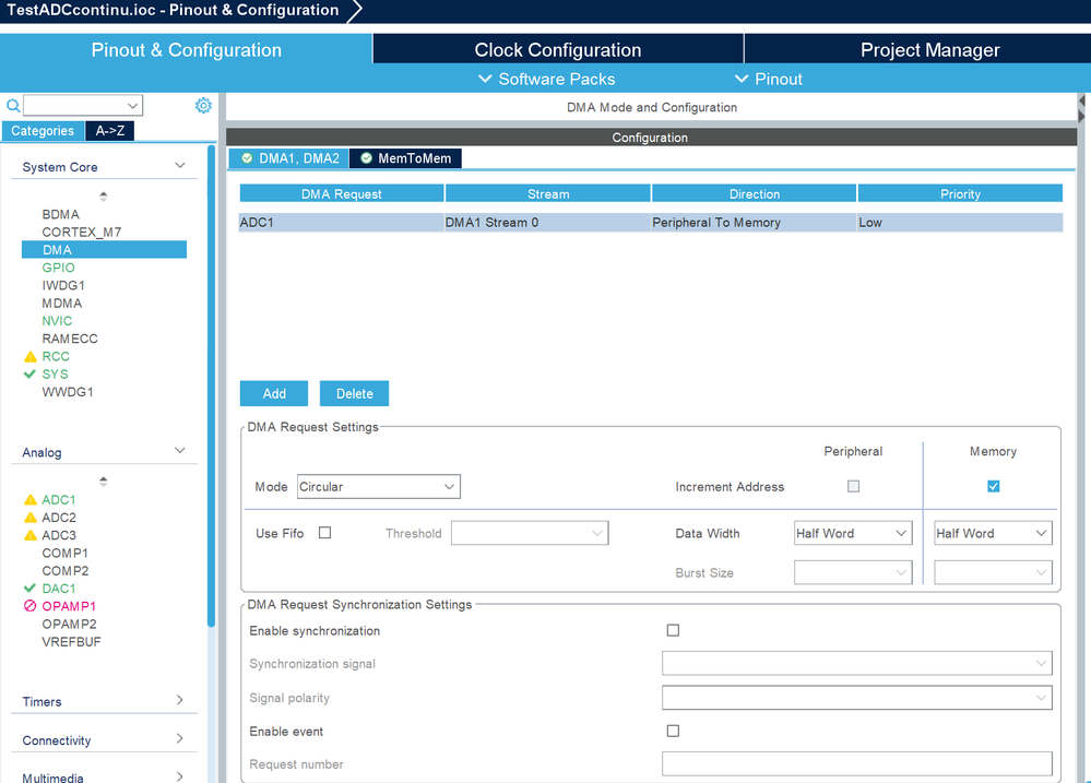
In order to use DMA just see at the device configuration tool, look at the available options there. First you should set up your device pins. Set the input pins. Then set the appropriate clock for the ADC peripheral to derive your sampling frequency from it. Then set the ADC clock divider to get the actual sampling frequency. Set the sampling resolution if selectable. Then go to the DMA tab and enable a channel that maps peripheral to memory. I used circular buffer and half-word, because the data arrives in 16-bit words. Just try to figure it out on your own and test if you get any data in the buffer. BTW, I used DMA to collect raw samples to filter an average reading and have some control over the signal to noise ratio. It's also a simple way to test if it works. Just connect some constant voltage (like 1V) to the ADC input, fill the buffer, then calculate the average value. If it roughly matches the voltage, then it works. At least it samples the voltage more or less correctly in terms of its value.
If you need more than just reading a value, then it's easier to start from where you already have some readings.
AFAK using ADC in STM32H7 doesn't require any additional middleware, all required settings and drivers are already built in the standard firmware package in STM32CubeIDE. Configuration of the DMA using STM32Cube IDE is pretty straight forward, I haven't even used any tutorial for it. I just used the FAFO method ;)
- Mark as Read
- Mark as New
- Bookmark
- Permalink
- Email to a Friend
- Report Inappropriate Content
Hello HTD,
So I followed the tutorial (getting started with ADC) step by step.
For reading a one time shot value from ADC it works fine:
I create the DAC and ADC:
Code:
/* USER CODE BEGIN 2 */
  int value_dac=0;
  HAL_DAC_Start(&hdac1, DAC_CHANNEL_2);//be sure to manually write the correct DAC channel
  float voltage=0;
  int value_adc=0;

  /* USER CODE END 2 */

  /* Infinite loop */
  /* USER CODE BEGIN WHILE */
  while (1)
  {
	  if (value_dac < 4095-200) {
	  	value_dac+=200;
	  } else {
	  	value_dac=0;
	  }
	  HAL_DAC_SetValue(&hdac1, DAC_CHANNEL_2, DAC_ALIGN_12B_R, value_dac);

	  HAL_Delay(1000);

	  HAL_ADC_Start(&hadc1);
	  HAL_ADC_PollForConversion(&hadc1, HAL_MAX_DELAY);
	  value_adc= HAL_ADC_GetValue(&hadc1);

	  HAL_Delay(1000);

	  voltage=value_dac*0.8;
        printf("DAC: %d (voltage %f) ADC: %d \r\n",value_dac,voltage,value_adc);


    /* USER CODE END WHILE */

    /* USER CODE BEGIN 3 */
  }
Result from printf/UART:
DAC: 200 (voltage 160.000000) ADC: 265 <\r><\n>
DAC: 400 (voltage 320.000000) ADC: 464 <\r><\n>
DAC: 600 (voltage 480.000000) ADC: 665 <\r><\n>
DAC: 800 (voltage 640.000000) ADC: 864 <\r><\n>
DAC: 1000 (voltage 800.000000) ADC: 1057 <\r><\n>
DAC: 1200 (voltage 960.000000) ADC: 1256 <\r><\n>
DAC: 1400 (voltage 1120.000000) ADC: 1459 <\r><\n>
DAC: 1600 (voltage 1280.000000) ADC: 1659 <\r><\n>
Now, I want to use a DMA to continuously read from the ADC.
As a first step I don't use a buffer but still one int for value_adc and it should get updated as the tutorial suggests.
I create the DMA and update the ADC. I don't change the DAC.
Code:
/* USER CODE BEGIN 2 */
  int value_dac=0;
  HAL_DAC_Start(&hdac1, DAC_CHANNEL_2);//be sure to manually write the correct DAC channel
  float voltage=0;
  int value_adc=0;

  HAL_ADCEx_Calibration_Start(&hadc1,ADC_CALIB_OFFSET,ADC_SINGLE_ENDED);
  HAL_ADC_Start_DMA(&hadc1,(uint32_t*)&value_adc,1);

  /* USER CODE END 2 */

  /* Infinite loop */
  /* USER CODE BEGIN WHILE */
  while (1)
  {
	  if (value_dac < 4095-200) {
	  	value_dac+=200;
	  } else {
	  	value_dac=0;
	  }
	  HAL_DAC_SetValue(&hdac1, DAC_CHANNEL_2, DAC_ALIGN_12B_R, value_dac);

	  HAL_Delay(1000);


	  HAL_Delay(1000);

	  voltage=value_dac*0.8;
        printf("DAC: %d (voltage %f) ADC: %d \r\n",value_dac,voltage,value_adc);


    /* USER CODE END WHILE */

    /* USER CODE BEGIN 3 */
  }
Result
DAC: 200 (voltage 160.000000) ADC: 0 <\r><\n>
DAC: 400 (voltage 320.000000) ADC: 0 <\r><\n>
DAC: 600 (voltage 480.000000) ADC: 0 <\r><\n>
DAC: 800 (voltage 640.000000) ADC: 0 <\r><\n>
DAC: 1000 (voltage 800.000000) ADC: 0 <\r><\n>
DAC: 1200 (voltage 960.000000) ADC: 0 <\r><\n>
So I guess the value_adc doesn't get update. I guess there is missing some kind of trigger to say that it should be updated with the DMA.
- Mark as Read
- Mark as New
- Bookmark
- Permalink
- Email to a Friend
- Report Inappropriate Content
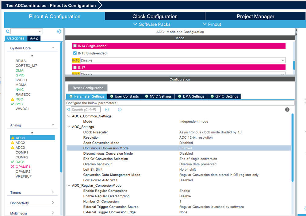
It seems like you need "Continuous conversion mode" enabled:
Then, using DMA I don't use HAL function to read value. I just start reading with HAL, then I read the data directly from my buffer.
I set the callback to be notified when the conversion is complete:
HAL_ADC_RegisterCallback(m_hadc, HAL_ADC_CONVERSION_COMPLETE_CB_ID, conversionComplete);Inside the function `conversionComplete` I just calculate the average from all samples in the buffer and trigger another notification when it's done. Of course instead of averaging the values you can do anything else with them, like copy them somewhere else.
I would paste my code but it's unnecessarily complex because it handles multiple channels and performs additional calculations, also it's done in C++. The only important part is the function takes `ADC_HandleTypeDef` as the only parameter. As this is an ISR, whatever you do in that function must be done very quickly, without blocking or god forbid waiting. So using UART from it is a no-no. It only averages the values and sets a variable that tells the other thread in my code that the new value is ready to be read. Then the other thread just reads the result. So in case of no OS used - your main thread is your main loop. It can loop and test if you set a special variable that the value is ready, when it's ready read it and send it to the UART, then clear the flag and loop. The callback mentioned earlier is responsible for actual reading exactly when the data from ADC is ready. Remember to not block / wait in callback, otherwise you would deadlock the MCU and it won't work.
- Mark as Read
- Mark as New
- Bookmark
- Permalink
- Email to a Friend
- Report Inappropriate Content
Yes I put the "Continuous conversion mode" enabled in my second example.
I used UART but if comment it and read by the debugger the value_adc variable it is still 0.
I also tried the
HAL_ADC_RegisterCallback
function be it is never called.
- Mark as Read
- Mark as New
- Bookmark
- Permalink
- Email to a Friend
- Report Inappropriate Content
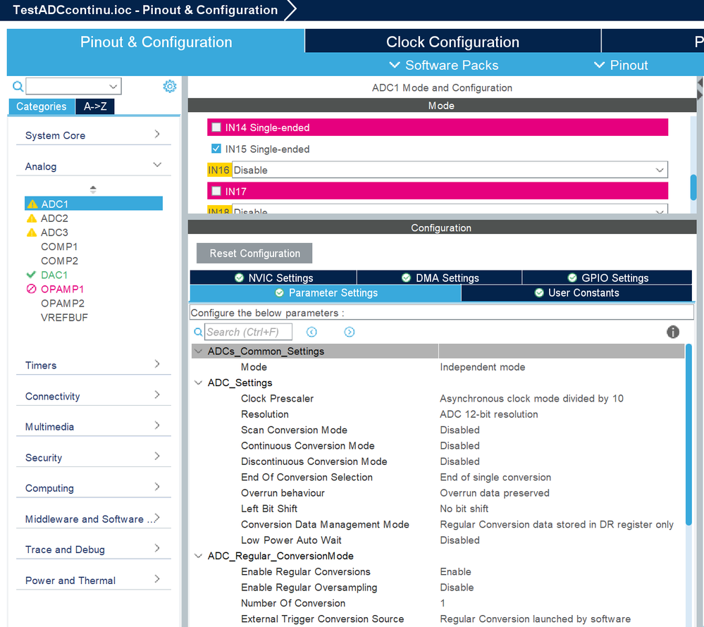
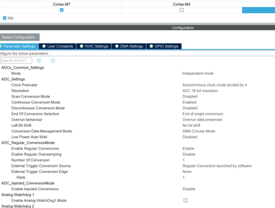
Looking at your screenshot, you have `Conversion Data Management Mode` set to `Regular Conversion data stored in DR register only`, I believe it should be set to `DMA Circular Mode`.
Here's how it's set in my project:
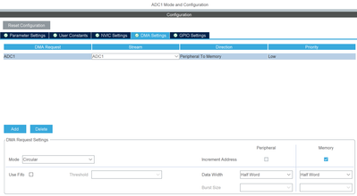
BTW, try to use more than 1 word for the data, define a buffer for like 128 samples as array. If your resolution is set to 12 bits, that the closest word size will be 16-bits. So I would use an array of let's say 128 of `uint16_t`, the length of the data should be 128 (number of 16-bit words). That's what I believe is half word in DMA settings, here:
Also be sure to have IRQ enabled:
Then the registered callback function should start to be called. And the elements of the buffer array should contain the measured values. I guess the main point of using DMA here is to quickly get many samples without interrupting MCU. So if you set like 128 samples (buffer size) - you will get the interrupt and the callback called when all of the samples are written in the buffer, so not on the single reading, but when multiple readings complete. IDK, maybe it would just work on a single value, but I haven't tested it. Try to replace single value with a buffer (and best make it length divisible by 4), then in the callback try to calculate the average of the values in the buffer, then copy result to another variable. Then in your main loop just print this value using UART debugger function. Please tell me if it worked.
- Mark as Read
- Mark as New
- Bookmark
- Permalink
- Email to a Friend
- Report Inappropriate Content
Silly me, I just saw the parameter you pointed out : 'Conversion Data Management Mode' to `DMA Circular Mode`. I guess this is the new parameter corresponding to the "DMA continuous request" from the outdated tutorial I was looking for.
When I choose this option, then my variable "value_adc" is updated correctly.
I replaced it with a buffer and the buffer was filled correctly too. There was a trick though, to declare as uint16_t buffer_adc[N] but then casted it as (uint32_t*)&buffer_adc, otherwise the buffer is filled weirdly.
However, I didn't use your callback function "HAL_ADC_RegisterCallback", but I use the functions explained in some other tutorials HAL_ADC_ConvHalfCpltCallback and HAL_ADC_ConvCpltCallback and it is correctly called.
Thank you for the help !
- Mark as Read
- Mark as New
- Bookmark
- Permalink
- Email to a Friend
- Report Inappropriate Content
I'm glad it worked ;) I forgot to tell that `HAL_ADC_RegisterCallback` is just a special way to do it, but it's not available until you enable it in STM32CubeIDE Project Manager / Advanced Settings / Register Callbacks / ADC. Most HAL peripherals can be set up to either use weak function overrides to provide callbacks, or register any (matching) function as callback. Each setting has its pros and cons. Registering callbacks allows easier integration with C++ code, overwriting the weak function is just overall simpler and more straight forward to do in C.
- Mark as Read
- Mark as New
- Bookmark
- Permalink
- Email to a Friend
- Report Inappropriate Content
I've been trying to get the LPUART working with the BDMA module on a STM32H7A3 using the information in this conversation along with the reference manual. I can TX characters byte by byte using polling and can see them on the logic analyzer but when I try to TX using the BDMA module, no characters are showing up on the logic analyzer. I have been using DMA with regular UARTs and the character match functionality for a while so I understand the basic concepts but still haven't gotten the LPUART working with the BDMA module. The whole problem is described in detail here https://community.st.com/t5/stm32-mcus-products/stm32h7a3-lpuart-and-bdma/m-p/623558#M231216 and I'm hoping to get a little more help here.
Thanks - Gene
- Mark as Read
- Mark as New
- Bookmark
- Permalink
- Email to a Friend
- Report Inappropriate Content
For anyone trying Solution example 2: Placing buffers in separated memory part, remember that by default RAM_D2 is not powered on.
To make this example work I had to add this to the start of main:
__HAL_RCC_D2SRAM1_CLK_ENABLE();
And because it isn't part of the normal MCU initialization, any data mapped to this section will NOT be initialized. So, for me, it was easiest to only place my receive buffer in RAM_D2.
And here is my CubeMx setup:
- Mark as Read
- Mark as New
- Bookmark
- Permalink
- Email to a Friend
- Report Inappropriate Content
Solution 3 solved my problem
Thank you, very useful
