VREF+ drops when DAC is used (STM32G0)
- Mark as New
- Bookmark
- Subscribe
- Mute
- Subscribe to RSS Feed
- Permalink
- Email to a Friend
- Report Inappropriate Content
2021-02-13 9:29 AM
I use a LM4040 voltage reference IC to generate a 3.00V reference voltage for the STM32G0 VREF+ pin. The resistor is 750 ohms, so 4mA can be sourced to the VREF+ pin (the datasheet specifies a minimum of 500 uA).
I use the STM32G0 DAC (channel 1 only), which is connected to a TLV172IDBVR op amp. The op amp data sheet indicates that its input bias current is only 10 pA, so I have to suppose that the DAC can easily drive it.
When I set the DAC to a high value, say 3500 (out of 4095), the VREF+ pin reads very close to 3.00V, as expected. But when I set the DAC value to a lower value such as 0, the VREF+ pin drops to 2.875V. Since the VREF+ is no longer stable, all ADC computations that I do afterwards are off.
Does anyone know what could cause the VREF+ pin to drop its voltage?
Thank you !
- Labels:
-
DAC
-
STM32G0 Series
- Mark as New
- Bookmark
- Subscribe
- Mute
- Subscribe to RSS Feed
- Permalink
- Email to a Friend
- Report Inappropriate Content
2021-02-13 6:04 PM
Hello
If vcc is 3.3v and the 750 ohm resistor is connected between Vcc and cathode of LM4040 (3.00V) then the maximum current can source without voltage drop is I= (Vcc-Vref)/Rs or (3.3-3)/750= 0.4mA 400μA.
Sugest to decrease Rs taking also in account the static power consumption of this complex.
- Mark as New
- Bookmark
- Subscribe
- Mute
- Subscribe to RSS Feed
- Permalink
- Email to a Friend
- Report Inappropriate Content
2021-02-13 7:46 PM
- Mark as New
- Bookmark
- Subscribe
- Mute
- Subscribe to RSS Feed
- Permalink
- Email to a Friend
- Report Inappropriate Content
2021-02-15 9:11 AM
Unfortunately, this is still a mystery because I experience VREF+ voltage drop even when pushing the LM4040 almost to its limit.
I decided to use a 27 ohms resistance, which should allow a current of 0.3 / 27 = 11 mA to flow through the VREF+ pin as well as the LM4040. My understanding is that the LM4040 will sink whatever current will not be used by the MCU.
Strangely, the VREF+ pin now reads 2.995 when the DAC output is set to 0, and 2.923 when the DAC is set to 4000. So it is the reverse situation I had when I was allowing less current to flow through VREF+.
Any clue?
- Mark as New
- Bookmark
- Subscribe
- Mute
- Subscribe to RSS Feed
- Permalink
- Email to a Friend
- Report Inappropriate Content
2021-02-15 11:45 AM
Hello
can you provide a schematic? which device are you refer? Note that VDDA must be >= vref.
VREFBUF also must be disabled to provide external voltage reference.
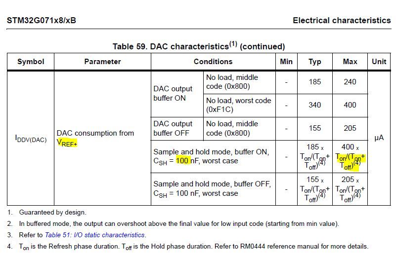
Vref consumption depends also from load capacitance connected to output.(dynamic condition)
In some devices is possible the internal PU/PD resistors to be connected to pin , independently from DAC config.
Make sure that DAC output pin is set to analog mode before DAC is enabled.
Consumption also depend from DAC output buffer state. (Buffer acts like Op-Amp configured as voltage follower).
Try to disconnect external opamp to isolate the problem of increased consumption.

- Mark as New
- Bookmark
- Subscribe
- Mute
- Subscribe to RSS Feed
- Permalink
- Email to a Friend
- Report Inappropriate Content
2021-02-15 2:30 PM
ADC loads VREF+ too.
Try a simplified program which does nothing but set the DAC once and then goes to loop.
Observe VREF+ using oscilloscope. I suspect the consumption from it is pulsed; try filtering.
JW
- Mark as New
- Bookmark
- Subscribe
- Mute
- Subscribe to RSS Feed
- Permalink
- Email to a Friend
- Report Inappropriate Content
2021-02-16 2:04 PM
Many thanks to everyone for kindly answering.
My VREF+ voltage is now stable.
I removed from my circuit a ferrite bead that I had inserted between 3.3V and the LM4040 resistor. I do not understand because this ferrite bead has a resistance of less than 0.5 ohms, but impedance of 600 ohms at 100 Mhz. So somehow, it is as if the ferrite bead was blocking current although the 3.3V isn't a signal with high frequency (unless it carries too much noise??).
Also, I removed the DAC buffering, it led to more precise ADC capture afterwards.
Many thanks to everyone again, your help has been much appreciated.
JL
- Mark as New
- Bookmark
- Subscribe
- Mute
- Subscribe to RSS Feed
- Permalink
- Email to a Friend
- Report Inappropriate Content
2021-02-16 2:26 PM
Thanks for coming back with the solution.
What capacitance do you have on the VREF+ against VSSA?
> although the 3.3V isn't a signal with high frequency
How do you know? Did you observe it using oscilloscope (and appropriate probing - we're talking millivolts and hundreds of MHz)?
As I've said, the VREF+ consumption is probably heavily pulsed.
JW
- Mark as New
- Bookmark
- Subscribe
- Mute
- Subscribe to RSS Feed
- Permalink
- Email to a Friend
- Report Inappropriate Content
2021-02-16 2:44 PM
Serial regulators/reference allow higher output current than quiescent current. Consider if doing a redesign. Also do not use Y capacitors and have them with close to the pins.