- STMicroelectronics Community
- STM32 MCUs
- STM32 MCUs Products
- Re: Using CTS and RTS signals connected to the mcu...
- Subscribe to RSS Feed
- Mark Topic as New
- Mark Topic as Read
- Float this Topic for Current User
- Bookmark
- Subscribe
- Mute
- Printer Friendly Page
Using CTS and RTS signals connected to the mcu's NBLx pins
- Mark as New
- Bookmark
- Subscribe
- Mute
- Subscribe to RSS Feed
- Permalink
- Email to a Friend
- Report Inappropriate Content
2024-01-24 7:33 AM - edited 2024-01-24 7:35 AM
The schemes of a production circuit are given to me from another designer for being analyised. PCB board is a STM32F103VC based circuit.
When I was looking at the bootloader circuitry scheme I saw how RS232 bus seems to be connected to the UART1 microcontroller port.
This circuitry implements BOOT1 and BOOT0 connections. These pins are two bit combination that allows different boot option, depending of logic levels there. "There is one of the boot option, known as embedded bootloader, that allows FLASH reprograming using UART1 port", datasheet says.
Up to here, seems to be clear and correct.
But diving a bit more I looked for what pins where exactly connected here, and they were these by one side (RX and TX on P9:P10:(
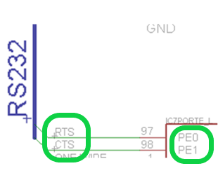
And these by the other side:
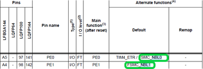
But if you look at datasheet tables you can see how PE0 and PE1 pins can only be GPIO floating inputs or they can be FSCM NABLx pins.
I think they should be here (PA11 and PA12) instead; because datasheet doesn't show any remap for USART1 anywhere else:
So I asked to my colleague whether the connection of RTS and CTS to PE0/1 where intentional. He told me that he was using the same solution as an old STM demo board, some years ago. I don't know what board is.
Rapidly I thought, if ST and my colleague are using this solution without problem, this means it works. But I'm unable to understand how the bootloader could program the flash using uart1 with CTS and RTS not being connected to UART1 corresponding pins. I don't find any explanation, not on datasheet neither googling.
I don't work with this peripheral (FSCM) before, I only know that NBLx pins they are used for enabling 8 bit access to SRAM or something like that.
Can anyone help me with this?
Solved! Go to Solution.
Accepted Solutions
- Mark as New
- Bookmark
- Subscribe
- Mute
- Subscribe to RSS Feed
- Permalink
- Email to a Friend
- Report Inappropriate Content
2024-01-24 7:50 AM
It looks as if we are currently only talking about the bootloader via UART, right? The AN2606 gives detailed explanations in section 15, according to which only PA9 and PA10 are used by UART1, RTS/CTS are not used.
Hope that answers your question?
Regards
/Peter
- Mark as New
- Bookmark
- Subscribe
- Mute
- Subscribe to RSS Feed
- Permalink
- Email to a Friend
- Report Inappropriate Content
2024-01-24 8:19 AM
So, acording to you RTS and CTS signals on my scheme are surelly used for another kind of things.
It's using flux control signals for FCSM control..
- Mark as New
- Bookmark
- Subscribe
- Mute
- Subscribe to RSS Feed
- Permalink
- Email to a Friend
- Report Inappropriate Content
2024-01-24 9:34 AM
Correct. For a better assessment, you would need to know the relevant circuit components and the function of the overall system.
Good luck!
/Peter
- After firmware flash, first time STOP 3 mode power consumption is higher (if board is not power cycled) in STM32 MCUs Products
- I2S bits rotated in STM32 MCUs Products
- Copy firmware from one STM32 MCU to another using STM32_Programmer_CLI.exe in STM32 MCUs Embedded software
- extremely slow sdram read write performance in STM32 MCUs Products
- STM32F747XIH6 ST-Link Connection Issue – Unable to Flash Code in Others: STM32 MCUs related


