- STMicroelectronics Community
- STM32 MCUs
- STM32 MCUs Products
- Strange behavior writing to external SRAM
- Subscribe to RSS Feed
- Mark Topic as New
- Mark Topic as Read
- Float this Topic for Current User
- Bookmark
- Subscribe
- Mute
- Printer Friendly Page
Strange behavior writing to external SRAM
- Mark as New
- Bookmark
- Subscribe
- Mute
- Subscribe to RSS Feed
- Permalink
- Email to a Friend
- Report Inappropriate Content
2019-07-29 1:31 AM
I have a STM32H753 with 16MByte, 32bit SDRAM and a Wiznet W5300 in 16bit mode (acts as SRAM Bank 1, SRAM_BANK_ADDR = 0x60000000).
So, if I read a Memory cell:
uint16_t aw = *(volatile uint16_t*)(SRAM_BANK_ADDR);all is ok. With a scope on NE1, NOE, NWE I got one read cycle on line NOE.
But if I write to the Memory cell:
*(volatile uint16_t*)(SRAM_BANK_ADDR) = 0x8000;I got four write cycles (shown on scope).
Going down to 8bit bus width, I got 8 write cycles.
This makes the W5300 confused.
But if I modify the Memory cell within the Debugger (Keil + ST-LinkV2, Memory Window)
I got one write cycle (as I expected).
Same code executed on a identical board assembled with a STM32F439 works perfect,
one write cycle as expected.
Does somebody has any idea to solve this Problem?
Best regards
Christian
- Labels:
-
STM32H7 Series
- Mark as New
- Bookmark
- Subscribe
- Mute
- Subscribe to RSS Feed
- Permalink
- Email to a Friend
- Report Inappropriate Content
2019-07-29 3:36 AM
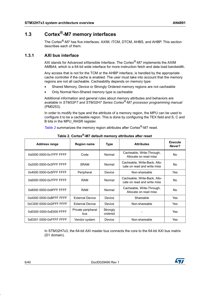
How's caching set up for that area in MPU?
JW
- Mark as New
- Bookmark
- Subscribe
- Mute
- Subscribe to RSS Feed
- Permalink
- Email to a Friend
- Report Inappropriate Content
2019-07-29 4:53 AM
I think Cache is disabled and commented out. Or is there any other Cache enabled by default on power up?
  /* Enable I-Cache---------------------------------------------------------*/
  //SCB_EnableICache();

  /* Enable D-Cache---------------------------------------------------------*/
  //SCB_EnableDCache();
I am new on this device. We used the STM32F439 before. The Manual of the H7 device have twice the amount of pages of the F439 device.
So I am (not) familiar with all details of this device.
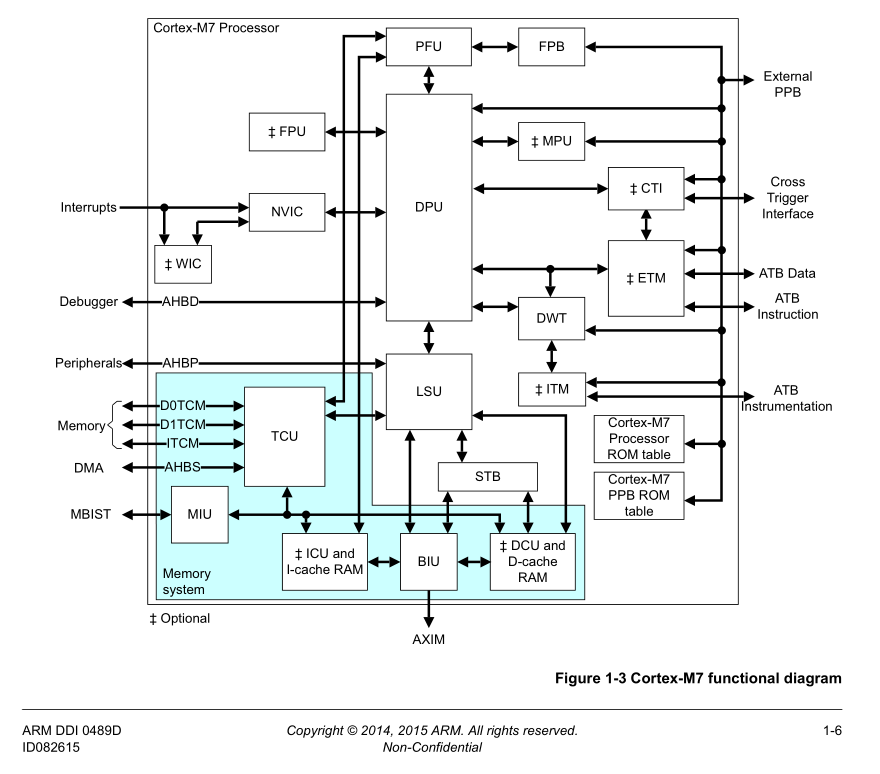
I think there is a relation between AXI buswidth (64 bit) and connected Memory. One write command generates 64bit/MEMBUSWIDTH writepulses on the NWE-line.
But why can I write to a single Memory cell with the Debugger?
Best regards
Christian
- Mark as New
- Bookmark
- Subscribe
- Mute
- Subscribe to RSS Feed
- Permalink
- Email to a Friend
- Report Inappropriate Content
2019-07-29 6:12 AM
> is there any other Cache enabled by default on power up?
I don't know. I don't use the 'H7.
> The Manual of the H7 device have twice the amount of pages of the F439 device.
That's no excuse. ;)
And you should add all the pages of the generic Cortex-M7 documentation.
> I think there is a relation between AXI buswidth (64 bit) and connected Memory.
Well spotted.
From Supported memories and transactions subchapter of the FMC chapter:
The memory region MPU attribute must be configured as “Device�? or “strongly-ordered�?
in order to prevent issues on devices that do not have the byte select feature. As an
example, if byte accesses are performed to 16-bit memories with the MPU attribute set
to “Normal memory�?, the AXI transaction size is 64 bits and the FMC splits the
transaction into four consecutive accesses while only one access is expected instead
of four.
> But why can I write to a single Memory cell with the Debugger?
Debugger may have it's own way to access the buses. Again, I don't use the 'H7 nor any Cortex-M7 device so I'm not familiar with the intimate details of its architecture.
JW
- STM32WL3 status when wakeup from deep sleep not working in STM32 MCUs Wireless
- Writing and reading external parallel flash with STM32 in STM32 MCUs Products
- Calling Touchgfx Thread during writing to external flash? in STM32 MCUs TouchGFX and GUI
- External Memory Byte Access in STM32 MCUs Products
- STM32H7RSxx OTG strange behavior with bulk transfer in STM32 MCUs Products

