- STMicroelectronics Community
- STM32 MCUs
- STM32 MCUs Products
- STM32L0x2: Combine two comparator outputs
- Subscribe to RSS Feed
- Mark Topic as New
- Mark Topic as Read
- Float this Topic for Current User
- Bookmark
- Subscribe
- Mute
- Printer Friendly Page
STM32L0x2: Combine two comparator outputs
- Mark as New
- Bookmark
- Subscribe
- Mute
- Subscribe to RSS Feed
- Permalink
- Email to a Friend
- Report Inappropriate Content
2019-10-30 6:37 AM
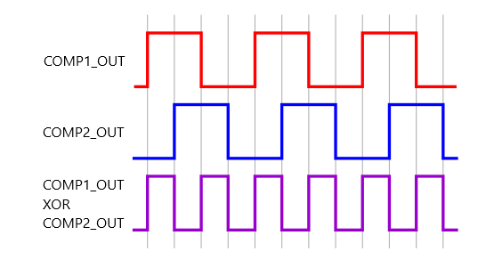
I have a STM32L072KB microcontroller and want to combine two analog signals (they represent a kind of "quadrature encoded signal" with a 50% duty cycle) into one "combined digital output signal", which have the doubled frequency (for my purpose the doubled output signal is used to provide the doubled accuracy)

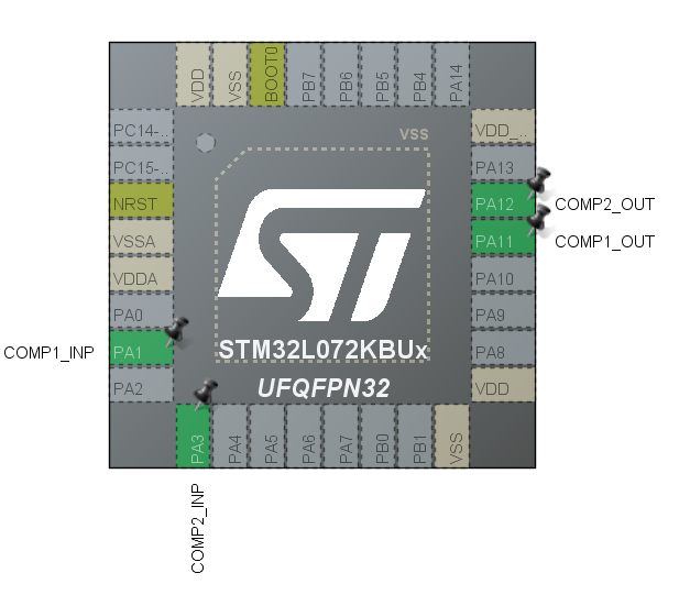
- COMP1_OUT -> PA11
- COMP2_OUT -> PA12
Due to my HW layout, I want to realize something like this configuration:
- COMP1_OUT ⊕ COMP2_OUT -> PA11
or
- COMP1_OUT ⊕ COMP2_OUT -> PA12
I have not found a way to directly connect both comparator outputs into one single output pin without introducing an SW/ISR delay/latency. I read that some general purpose timers offer a so called "Hall" encoder mode, which supports XOR-ing up to 3 input signals. But since connecting a Timer directly to a GPIO via DMA seems to be impossible on a STM32L0-core, I have no idea how to implement this...
Does anyone know a "hardware/fast way" to route/XOR simultaneously both COMP_OUTs of a STM32L0x2 to a single GPIO output pin (either PA11 or PA12) or is it in that case inevitable, to use an ISR-based solution (the HW-layout is fixed and cannot be changed)?
- Labels:
-
COMP
-
STM32L0 Series
- Mark as New
- Bookmark
- Subscribe
- Mute
- Subscribe to RSS Feed
- Permalink
- Email to a Friend
- Report Inappropriate Content
2019-11-03 1:31 PM
Maybe this could be pulled out by
- setting TIM2_OR.TI4_RMP to 0b01: TIM2 TI4 input connected to COMP2_OUT
- setting CH4 in TIM2_CCMR2 to input capture from its "native" input,
- setting CH4 to capture at both edges in TIM2_CCER by setting both CC4P and CC4NP
- enabling CH4 by setting CC4E
- enabling DMA requests from CH4 by setting TIM4_DIER.CC4DE
- selecting TIM2_CH4 as trigger for DMA channel 4
- setting up DMA channel 4 to DMA from a buffer in memory to COMP1_CSR, circular mode, NDTR set to 2
- storing to the buffer in memory from which DMA runs, values for COMP1_CSR so that they have alternating values for COMP1POLARITY
and that's roughly it.
It is a bit fragile in that it needs to be started when COMP2OUT has the proper polarity, and edges in COMP2 must be far enough apart each other so that the whole mechanism succeeds to write the proper value into COMP1_CSR for each edge.
JW
- Output Compare Register update in stm32 in STM32CubeMX (MCUs)
- Timer Output Compare example TIM_OCActive in STM32 MCUs Embedded software
- Dac -> COMP -> Timer -> DMA -> dual SPI_TX in STM32 MCUs Products
- STM32G474 HRTIMER ADC Trigger in STM32 MCUs Products
- Change timers output compare mode in STM32 MCUs Products
