- STMicroelectronics Community
- STM32 MCUs
- STM32 MCUs Products
- STM32H7 SPI DMA not working
- Subscribe to RSS Feed
- Mark Topic as New
- Mark Topic as Read
- Float this Topic for Current User
- Bookmark
- Subscribe
- Mute
- Printer Friendly Page
STM32H7 SPI DMA not working
- Mark as New
- Bookmark
- Subscribe
- Mute
- Subscribe to RSS Feed
- Permalink
- Email to a Friend
- Report Inappropriate Content
2021-01-14 04:58 AM
Hello,
When I use DMA with SPI it is not working.

void HAL_GPIO_EXTI_Callback(uint16_t GPIO_Pin)
{
	if(GPIO_Pin == DRDY_ADC_Pin)
	{
		HAL_SPI_Receive_DMA(&hspi1, SPI1_RxBuffer, READBACK_LENGTH);
	}
}
SPI1 RX Buffer is located in a DMA accessible memory, RAM D2 (it works I checked the .map) :
uint8_t __attribute__(( section(".ramd2section"))) SPI1_RxBuffer[READBACK_LENGTH]; // SPI TxMy question is do I need to use a setup function outside of what HAL_SPI_MspInit() already does. For example HAL_MDMA_Start_IT() ?
I've red few posts with the same problem but the solution is never explicated or done not using only HAL function.
What I use :
SPI1 Master full-duplex
DMA1 Stream 2 SPI1_Rx to SPI1_RxBuffer
MDMA Stream 0 SPI1_RxBuffer to ads_buf located in DTCMRAM
- Labels:
-
DMA
-
SPI
-
STM32H7 Series
- Mark as New
- Bookmark
- Subscribe
- Mute
- Subscribe to RSS Feed
- Permalink
- Email to a Friend
- Report Inappropriate Content
2021-01-14 05:24 AM
Read out and check/post SPI and relevant DMA registers (including status) content.
JW
- Mark as New
- Bookmark
- Subscribe
- Mute
- Subscribe to RSS Feed
- Permalink
- Email to a Friend
- Report Inappropriate Content
2021-01-14 05:31 AM
Tried adding DMAMUX init but it didnt change anything
dmamux_ReqGenParams.SignalID  = 37U;
dmamux_ReqGenParams.Polarity  = HAL_DMAMUX_REQ_GEN_RISING;
dmamux_ReqGenParams.RequestNumber = 1;

HAL_DMAEx_ConfigMuxRequestGenerator(&hdma_spi1_rx,&dmamux_ReqGenParams);

/* NVIC configuration for DMAMUX request generator overrun errors*/
HAL_NVIC_SetPriority(DMAMUX2_OVR_IRQn, 0, 1);
HAL_NVIC_EnableIRQ(DMAMUX2_OVR_IRQn);

HAL_DMAEx_EnableMuxRequestGenerator (&hdma_spi1_rx);- Mark as New
- Bookmark
- Subscribe
- Mute
- Subscribe to RSS Feed
- Permalink
- Email to a Friend
- Report Inappropriate Content
2021-01-14 05:37 AM
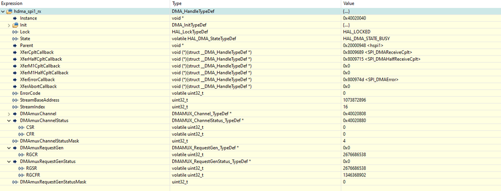
The SPI is always in "HAL_SPI_STATE_BUSY_RX"
I got this with debugging tool for the DMA Handler
- Mark as New
- Bookmark
- Subscribe
- Mute
- Subscribe to RSS Feed
- Permalink
- Email to a Friend
- Report Inappropriate Content
2021-01-14 01:54 PM
I mean the SPI and DMA peripherals (and, once you've mentioned, relevant DMAMUX) registers.
JW
- Mark as New
- Bookmark
- Subscribe
- Mute
- Subscribe to RSS Feed
- Permalink
- Email to a Friend
- Report Inappropriate Content
2021-01-15 12:43 AM
Here is my DMA init
hdma_spi1_rx.Instance = DMA1_Stream2;
    hdma_spi1_rx.Init.Request = DMA_REQUEST_SPI1_RX;
    hdma_spi1_rx.Init.Direction = DMA_PERIPH_TO_MEMORY;
    hdma_spi1_rx.Init.PeriphInc = DMA_PINC_DISABLE;
    hdma_spi1_rx.Init.MemInc = DMA_MINC_ENABLE;
    hdma_spi1_rx.Init.PeriphDataAlignment = DMA_PDATAALIGN_BYTE;
    hdma_spi1_rx.Init.MemDataAlignment = DMA_MDATAALIGN_BYTE;
    hdma_spi1_rx.Init.Mode = DMA_NORMAL;
    hdma_spi1_rx.Init.Priority = DMA_PRIORITY_LOW;
    hdma_spi1_rx.Init.FIFOMode = DMA_FIFOMODE_DISABLE;
    if (HAL_DMA_Init(&hdma_spi1_rx) != HAL_OK)
    {
      Error_Handler();
    }

    __HAL_LINKDMA(hspi,hdmarx,hdma_spi1_rx);

    /* SPI1 interrupt Init */
    HAL_NVIC_SetPriority(SPI1_IRQn, 0, 0);
    HAL_NVIC_EnableIRQ(SPI1_IRQn);
And my SPI init
hspi1.Instance = SPI1;
  hspi1.Init.Mode = SPI_MODE_MASTER;
  hspi1.Init.Direction = SPI_DIRECTION_2LINES;
  hspi1.Init.DataSize = SPI_DATASIZE_8BIT;
  hspi1.Init.CLKPolarity = SPI_POLARITY_LOW;
  hspi1.Init.CLKPhase = SPI_PHASE_2EDGE;
  hspi1.Init.NSS = SPI_NSS_SOFT;
  hspi1.Init.BaudRatePrescaler = SPI_BAUDRATEPRESCALER_256;
  hspi1.Init.FirstBit = SPI_FIRSTBIT_MSB;
  hspi1.Init.TIMode = SPI_TIMODE_DISABLE;
  hspi1.Init.CRCCalculation = SPI_CRCCALCULATION_DISABLE;
  hspi1.Init.CRCPolynomial = 0x0;
  hspi1.Init.NSSPMode = SPI_NSS_PULSE_DISABLE;
  hspi1.Init.NSSPolarity = SPI_NSS_POLARITY_LOW;
  hspi1.Init.FifoThreshold = SPI_FIFO_THRESHOLD_01DATA;
  hspi1.Init.TxCRCInitializationPattern = SPI_CRC_INITIALIZATION_ALL_ZERO_PATTERN;
  hspi1.Init.RxCRCInitializationPattern = SPI_CRC_INITIALIZATION_ALL_ZERO_PATTERN;
  hspi1.Init.MasterSSIdleness = SPI_MASTER_SS_IDLENESS_00CYCLE;
  hspi1.Init.MasterInterDataIdleness = SPI_MASTER_INTERDATA_IDLENESS_00CYCLE;
  hspi1.Init.MasterReceiverAutoSusp = SPI_MASTER_RX_AUTOSUSP_DISABLE;
  hspi1.Init.MasterKeepIOState = SPI_MASTER_KEEP_IO_STATE_DISABLE;
  hspi1.Init.IOSwap = SPI_IO_SWAP_DISABLE;
  if (HAL_SPI_Init(&hspi1) != HAL_OK)
  {
    Error_Handler();
}- Mark as New
- Bookmark
- Subscribe
- Mute
- Subscribe to RSS Feed
- Permalink
- Email to a Friend
- Report Inappropriate Content
2021-01-15 02:00 AM
I'm not really interested in source code, I don't use Cube and don't quite understand it.
Read out the registers' content.
JW
- Mark as New
- Bookmark
- Subscribe
- Mute
- Subscribe to RSS Feed
- Permalink
- Email to a Friend
- Report Inappropriate Content
2021-01-15 02:34 AM
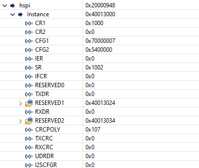
Sorry, I get it now. I looked register value with debugger tool at the end of the init function:
SP1 :
CR1 = 0x 0000 1000
CR2 = 0
CFG1 = 0x 7000 0007
CFG2 = 0x 0540 0000
IER = 0
SR = 0x 0000 1002
IFCR = 0
TXDR = 0
RXDR = 0
UDRDR = 0
I2SCFGR = 0
I got it from this :

// DMA
CR = 0x 0000 0400
FCR = 0x 0000 0020

// DMAMUX
CR = 0x 0000 0025
Do you think I should stop using Cube and just go with the datasheet ?
Thank you,
Gabriel
- Mark as New
- Bookmark
- Subscribe
- Mute
- Subscribe to RSS Feed
- Permalink
- Email to a Friend
- Report Inappropriate Content
2021-01-15 07:37 AM
I added my own "Bare Metal" register values :
#define DMAMUX_SPI1_RX_ID 37U
void SPI1_DMA1_DMAMUX_MDMA_init (void)
{
	//----Shutdown
	SPI1->CR1 = 0;
	DMAMUX1_Channel2->CCR = 0;
	DMA1_Stream2->CR = 0;
	MDMA_Channel2->CCR = 0;

	//------DMA1 Stream 2----

	// Configuration Register
	DMA1_Stream2->CR = DMA_SxCR_CIRC | DMA_SxCR_PL_0 | DMA_SxCR_PL_1 | DMA_SxCR_MINC | DMA_SxCR_TCIE;
	// Fifo control register
	DMA1_Stream2->FCR = 0;
	// Peripheral address register
	DMA1_Stream2->PAR = (uint32_t)&(SPI1->RXDR);
	// Memory address
	DMA1_Stream2->M0AR = (uint32_t)&(SPI1_RxBuffer[0]);
	// Second buffer in case of double buffer
	DMA1_Stream2->M1AR = 0;
	// Number of data items to transfer NDTR*PSIZE
	DMA1_Stream2->NDTR = READBACK_LENGTH;

	// Clear interrupt registers
	DMA1->LISR = 0x0F7D;
	DMA1->HISR = 0x0F7D;
	DMA1->LIFCR = 0x0F7D;
	DMA1->HIFCR = 0x0F7D;

	//------DMAMUX1 Channel 2----

	// Configuration Register
	DMAMUX1_Channel2->CCR = DMAMUX_CxCR_EGE | DMAMUX_SPI1_RX_ID;
	// Request Generator Configuration Register
	DMAMUX1_RequestGenerator2->RGCR = DMAMUX_RGxCR_GE | DMAMUX_RGxCR_GPOL_0 | 2U;

	// Clear interrupt registers
	DMAMUX1_ChannelStatus->CFR = 0x0000FFFF;
	DMAMUX1_RequestGenStatus->RGSR = 0x000000FF;
	DMAMUX1_RequestGenStatus->RGCFR = 0x000000FF;

	//------MDMA Channel 2----

	// Config Registers
	MDMA_Channel2->CCR = MDMA_CCR_PL_1 | MDMA_CCR_PL_0 | MDMA_CCR_TCIE | MDMA_CCR_CTCIE;
	MDMA_Channel2->CTCR = ((READBACK_LENGTH-1)CSAR = (uint32_t)&(SPI1_RxBuffer[0]);
	MDMA_Channel2->CDAR = (uint32_t)&(ads_buf[0]);
	MDMA_Channel2->CTBR = MDMA_CTBR_SBUS | MDMA_CTBR_SBUS | 2;
	// Clear interrupt
	MDMA_Channel2->CIFCR = 0x0000001F;

	// Configuration Register


	// Clear interrupt registers
	DMAMUX1_ChannelStatus->CFR = 0x0000FFFF;
	DMAMUX1_RequestGenStatus->RGSR = 0x000000FF;
	DMAMUX1_RequestGenStatus->RGCFR = 0x000000FF;

	//------SP1------

	// Configuration Registers
	SPI1->CR2 = (1<<16U) | READBACK_LENGTH;
	SPI1->CFG1 = (0x01110000) | SPI_CFG1_RXDMAEN;
	SPI1->CFG2 = SPI_CFG2_AFCNTR | SPI_CFG2_SSOE | SPI_CFG2_CPHA | SPI_CFG2_MASTER;
	SPI1->I2SCFGR = 0;
	// Clear interrupt registers
	SPI1->IFCR = 0x00000FF4;

	//Start Peripherals
	MDMA_Channel2->CCR |= MDMA_CCR_EN;
	DMAMUX1_Channel2->CCR |= DMAMUX_CxCR_EGE;
	DMA1_Stream2->CR |= DMA_SxCR_EN;
	SPI1->CR1 = SPI_CR1_SPE;
}
But the chronogram is still the exact same I posted before
- Mark as New
- Bookmark
- Subscribe
- Mute
- Subscribe to RSS Feed
- Permalink
- Email to a Friend
- Report Inappropriate Content
2021-01-15 03:39 PM
This appears to be much more complicated than I thought. I don't use the H7 and I realized that the SPI in there is much more different from other STM32 than I thought, and I don't understand how Rx-only on this SPI is supposed to work. It appears to me that there's no such mode in this SPI.
In other STM32, once you set Rx-only mode and set SPE, it automatically starts to generate clocks. Here, it appears, that you are supposed to Tx to be able to generate clocks.
JW
- How to trigger ADC at a specific point during the ON period of PWM in STM32F303ZE? in STM32 MCUs Products
- Internal SMPS efficiency (STM32WLE5) around 60%? in STM32 MCUs Products
- Not getting ADC ready signal (ADRDY bit) after enable STM32U5A5 in STM32 MCUs Embedded software
- stm32wb1mmc maximum number of services in STM32 MCUs Wireless
- Subject: Issues with LWIP on Nucleo-F746ZG – Release Mode & MPU Configuration in STM32 MCUs Products
