- STMicroelectronics Community
- STM32 MCUs
- STM32 MCUs Products
- STM32F4 FMC/FSMC Sub-Banks' Addresses/Offsets
- Subscribe to RSS Feed
- Mark Topic as New
- Mark Topic as Read
- Float this Topic for Current User
- Bookmark
- Subscribe
- Mute
- Printer Friendly Page
STM32F4 FMC/FSMC Sub-Banks' Addresses/Offsets
- Mark as New
- Bookmark
- Subscribe
- Mute
- Subscribe to RSS Feed
- Permalink
- Email to a Friend
- Report Inappropriate Content
2017-12-26 08:12 PM
Hello STers,
First of all, I would like to take this opportunity to wish you a Merry Christmas and a Happy New Year full of success and prosperity.
Well, as I'm starting to utilize the FMC/FSMC peripheral in one of my projects (interfacing a legacy chip), I have got some questions and would appreciate your help answering them.
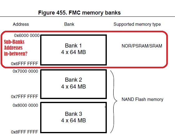
According to the datasheet (memory mapping), each bank is divided into 4-sub banks, 64 MBytes each.

Aside from the fact that each bank assigns a unique Chip Select signal (CS), I couldn't find any reference to how one could calculate the offsets of these banks?
For example,
0x6400 0000 is the base address for the second bank (NE2), but how was that obtained? I mean, adding 64MB to the base address of 0x60000000 has resulted to something around 67MB.
For writing/reading, I'm using the following functions:
uint8_t SRAM_ReadReg()
{ return *(uint8_t*)SRAM_ADDR; // Address defined earlier 0x60000000 }void SRAM_WriteReg(uint8_t RegValue)
{ *(uint8_t*)SRAM_ADDR = RegValue; }I have used the first bank (NE1) for these. Is there any better approach?
Thanks
Solved! Go to Solution.
Accepted Solutions
- Mark as New
- Bookmark
- Subscribe
- Mute
- Subscribe to RSS Feed
- Permalink
- Email to a Friend
- Report Inappropriate Content
2018-01-05 05:44 AM
1MB=0x10'0000
64MB=0x400'0000
Thus, 0x6000'0000+0x400'0000=0x6400'0000 for NE2-controlled bank.
0x6000'0000=1536MB=1.5GB
(It would be more correct to write
https://en.wikipedia.org/wiki/Mebibyte
/GiB)JW
- Mark as New
- Bookmark
- Subscribe
- Mute
- Subscribe to RSS Feed
- Permalink
- Email to a Friend
- Report Inappropriate Content
2018-01-05 11:26 AM
Yep, that was correct, and I got it now! I wasn't multiplying by 1048576 (1MB), therefore I got a wrong value. Now, 1024*1024 =
1048576 = 2^20.
1048576 * 64 = 67108864 = 0x4000000. When added to the base address, we get
0x64000000 for NE2.
Thanks